
SN74AHCT1G08 Single 2-Input Positive-AND Gate
The NYFEA SN74AHCT1G08 implements one 2-input positive-AND function in a five-terminal package. It operates from 2.0 V to 5.5 V, accepts TTL-voltage-compatible inputs, specifies partial-power-down Ioff, and is offered in SOT23-5 and SC70-5 packages for −40 °C to +125 °C operation.
Product scope: SN74AHCT1G08 is a combinational logic gate, not a voltage regulator, sequencer, latch, oscillator, level-shifter controller or safety monitor. It stores no state. Output Y is HIGH only while both A and B are interpreted as HIGH. Verify logic thresholds, output loading, edge rate, power sequencing and system fault behavior in the final design.
This page is an engineering selection summary. The controlled PDF remains the authority for limits, footnotes, package tolerances and production release.
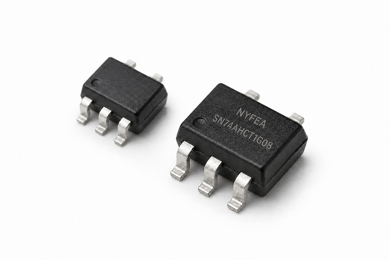
Product Overview and Selection Scope
SN74AHCT1G08 is a single-gate AHCT logic device for combining two positive-logic conditions. Its output is asserted only when both inputs meet the HIGH-level threshold. The device is optimized for operation around a 5 V logic rail while retaining a recommended VCC range of 2.0 V to 5.5 V.
- Single positive-AND gate: one A input, one B input and one Y output.
- TTL-voltage-compatible inputs: at VCC = 4.5 V to 5.5 V, VIH is 2.0 V minimum and VIL is 0.8 V maximum.
- Partial-power-down support: Ioff is specified with VCC = 0 V to help prevent backflow through the output path.
- Low static supply current: 0.1 µA typical at +25 °C under the stated ICC test condition; 10 µA maximum over the full operating range.
- Output drive: at VCC = 5.0 V and |IO| = 32 mA, VOH is 4.2 V minimum and VOL is 0.5 V maximum over the full temperature range.
- Wide ambient range: −40 °C to +125 °C.
- Compact options: SC70-5 and SOT23-5, both MSL3 and supplied on 3,000-piece tape-and-reel packaging.
- Green packages: the product description identifies both package options as Green.
Logic Function, Truth Table and Five-Pin Assignment
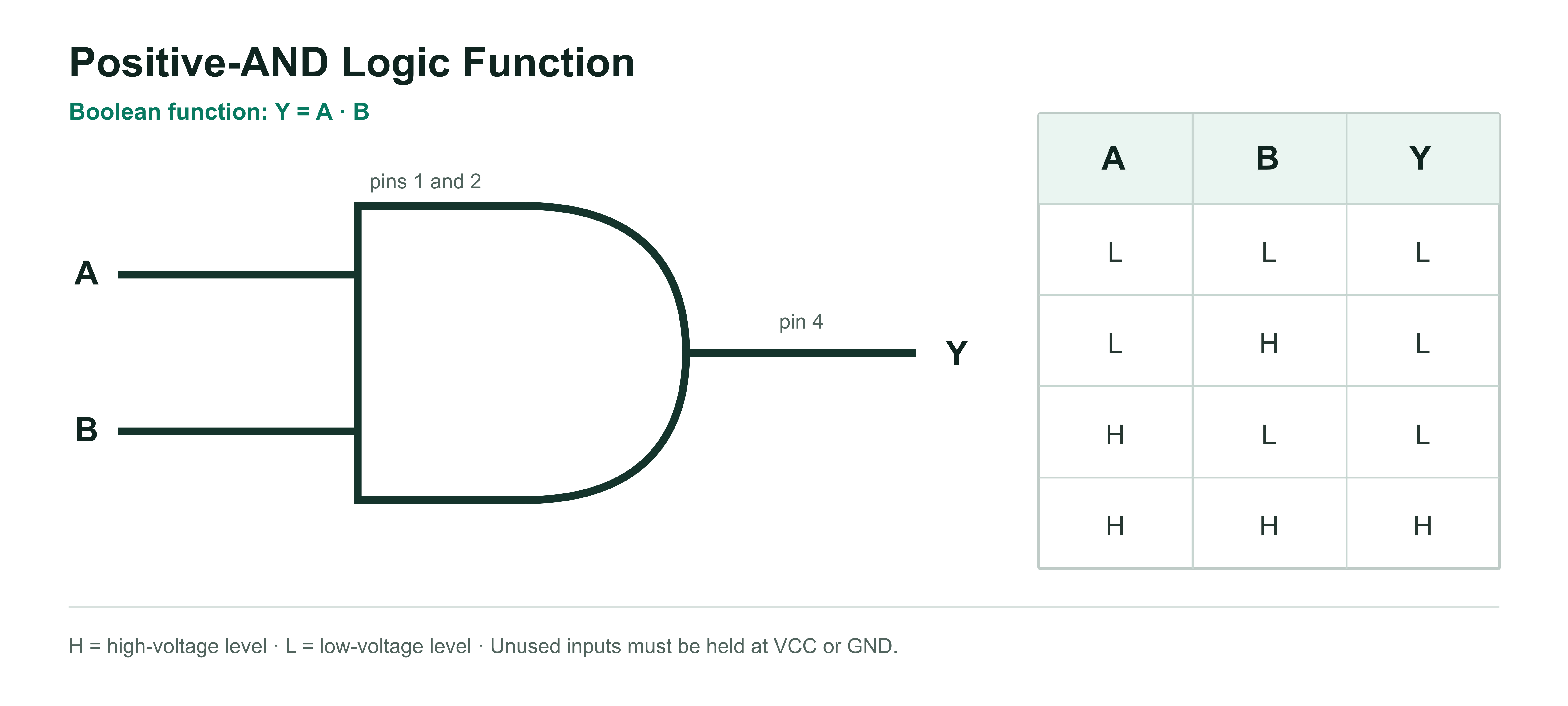
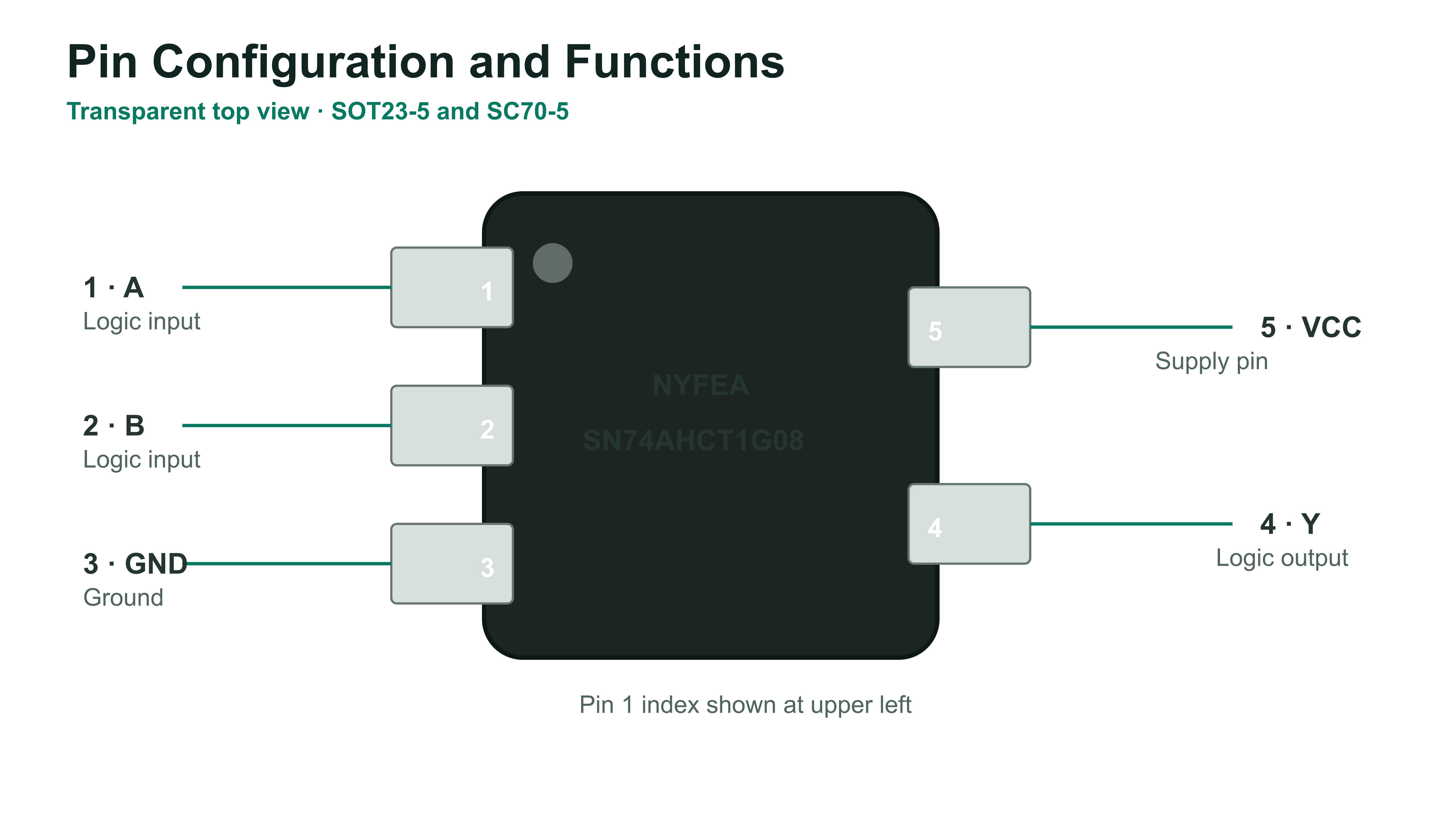
The Boolean function is Y = A · B. In positive logic, Y is HIGH only for A = HIGH and B = HIGH. The package pin assignment is common to both listed package options.
| Pin | Name | Type | Function | Design note |
|---|---|---|---|---|
| 1 | A | Input | Positive-logic input A | Do not leave floating. |
| 2 | B | Input | Positive-logic input B | Do not leave floating. |
| 3 | GND | Power | Ground reference | Connect to a low-impedance return. |
| 4 | Y | Output | AND-function output | Avoid bus contention and excessive capacitive loading. |
| 5 | VCC | Power | Supply input | Bypass locally to GND. |
Ordering Codes, Markings and Package Selection
Two orderable part numbers are listed. The electrical operating range is the same; the primary selection differences are package size, body tolerance and top marking.
| Orderable part number | Package | Package marking | MSL | Shipment | Temperature range |
|---|---|---|---|---|---|
| SN74AHCT1G08DCKR | SC70-5 | BEG | MSL3 | Tape and reel, 3,000 | −40 °C to +125 °C |
| SN74AHCT1G08DBVR | SOT23-5 | B08S | MSL3 | Tape and reel, 3,000 | −40 °C to +125 °C |
Recommended Operating Conditions and Absolute Limits
Recommended operating conditions define the region in which normal device operation is specified. Absolute maximum ratings are stress limits, not design operating points.
Recommended operating conditions
| Parameter | Symbol | Condition | Minimum | Maximum | Unit |
|---|---|---|---|---|---|
| Supply voltage | VCC | Operating | 2.0 | 5.5 | V |
| HIGH-level input voltage | VIH | VCC = 2.0 V | 1.0 | — | V |
| VCC = 3.3 V | 1.5 | — | |||
| VCC = 4.5 V to 5.5 V | 2.0 | — | |||
| LOW-level input voltage | VIL | VCC = 2.0 V | — | 0.3 | V |
| VCC = 3.3 V | — | 0.55 | |||
| VCC = 4.5 V to 5.5 V | — | 0.8 | |||
| Input voltage | VI | Recommended | 0 | 5.5 | V |
| Output voltage | VO | Recommended | 0 | VCC | V |
| Input transition rise or fall | Δt/Δv | VCC = 2.0 V to 5.5 V | — | 5 | ns/V |
| Operating free-air temperature | TA | — | −40 | +125 | °C |
Absolute maximum ratings
| Parameter | Condition | Minimum | Maximum | Unit |
|---|---|---|---|---|
| Supply voltage, VCC | Stress rating | −0.5 | 6.5 | V |
| Input voltage, VI | Stress rating | −0.5 | 6.5 | V |
| Output voltage, VO | High-impedance or power-off state | −0.5 | 6.5 | V |
| Output voltage, VO | HIGH or LOW state | −0.5 | VCC + 0.5 | V |
| Continuous output current | IO | −50 | +50 | mA |
| Continuous VCC or GND current | — | −100 | +100 | mA |
| Junction temperature | TJ | −65 | +150 | °C |
| Storage temperature | Tstg | −65 | +150 | °C |
DC Electrical Characteristics with Test Conditions
Voltage levels and current values are meaningful only together with VCC, load current and temperature. “Typical” values are characterization norms, not guaranteed limits.
Output HIGH and output LOW
| Parameter | Test current | VCC | Temperature | Guaranteed value | Unit |
|---|---|---|---|---|---|
| VOH | IOH = −100 µA | 2.0 V to 5.5 V | Full | Minimum VCC − 0.1 | V |
| VOH | IOH = −8 mA | 2.0 V | Full | Minimum 1.6 | V |
| VOH | IOH = −24 mA | 3.3 V | Full | Minimum 2.5 | V |
| VOH | IOH = −32 mA | 4.5 / 5.0 / 5.5 V | Full | Minimum 3.8 / 4.2 / 4.8 | V |
| VOL | IOL = 100 µA | 2.0 V to 5.5 V | Full | Maximum 0.1 | V |
| VOL | Source table prints IOH = 8 mA | 2.0 V | Full | Maximum 0.45 | V |
| VOL | Source table prints IOH = 24 mA | 3.3 V | Full | Maximum 0.55 | V |
| VOL | IOL = 32 mA | 4.5 / 5.0 / 5.5 V | Full | Maximum 0.55 / 0.50 / 0.45 | V |
Leakage, supply current and input capacitance
| Parameter | Test condition | VCC | Temperature | Typical | Maximum | Unit |
|---|---|---|---|---|---|---|
| Input current, II | A or B at 5.5 V or GND | 0 V to 5.5 V | +25 °C / full | ±0.1 / — | — / ±5 | µA |
| Power-off leakage, Ioff | VI or VO = 5.5 V | 0 V | +25 °C / full | ±0.1 / — | — / ±10 | µA |
| Supply current, ICC | VI = 5.5 V or GND; IO = 0 | 2.0 V to 5.5 V | +25 °C / full | 0.1 / — | — / 10 | µA |
| Additional supply current, ICCT | One input at 3.4 V; other input at VCC or GND | 5.5 V | Full | — | 500 | µA |
| Input capacitance, Ci | VCC = 0 V; f = 10 MHz | 0 V | +25 °C | 6 | — | pF |
AC Switching Characteristics and Measurement Conditions
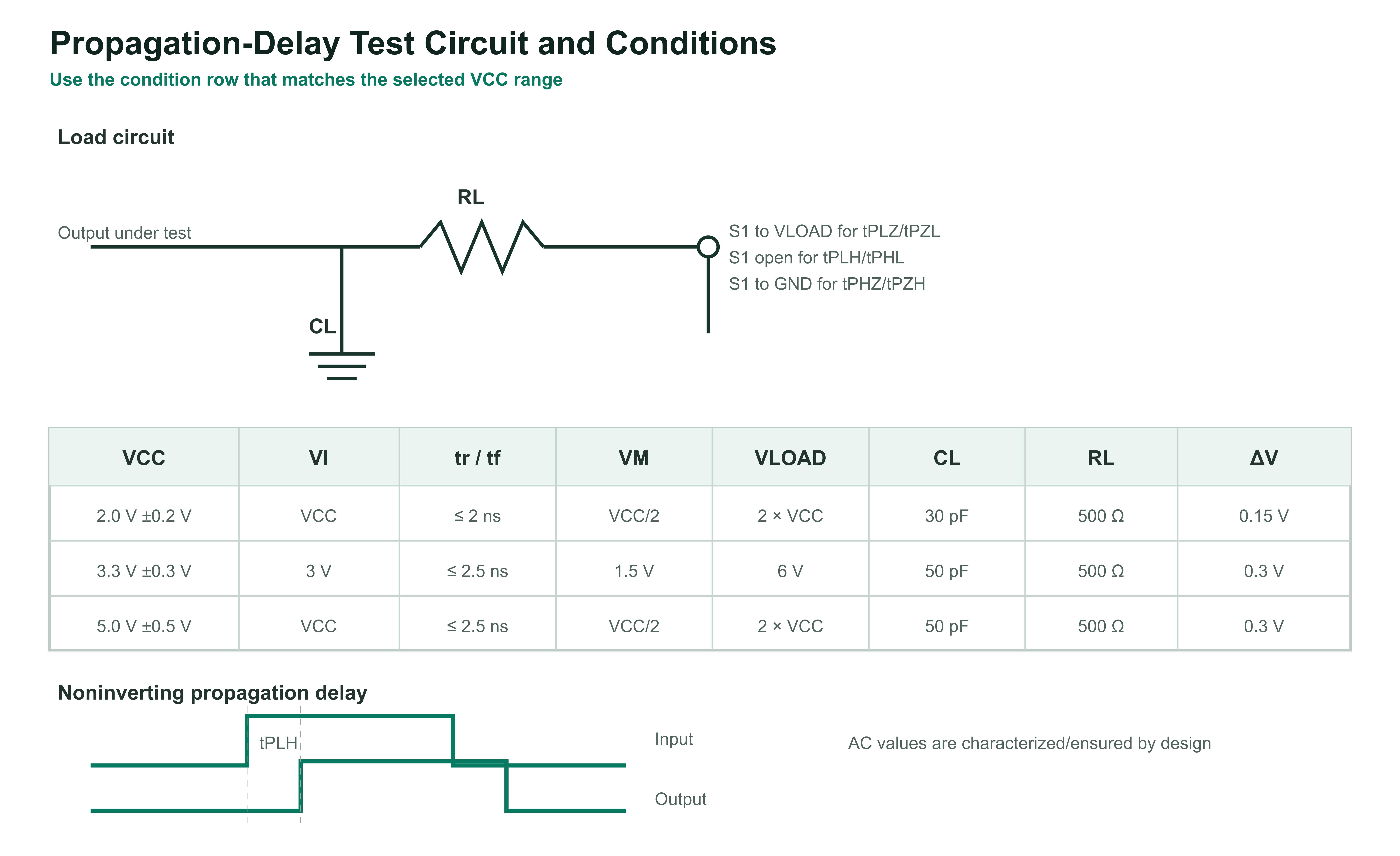
The AC table lists typical propagation delay and power-dissipation capacitance. The specification states that these values are ensured by design and/or characterization and are not production tested.
| Parameter | VCC | Load | Typical | Unit | Status |
|---|---|---|---|---|---|
| Propagation delay, tpd | 2.0 V ±0.2 V | CL = 30 pF; RL = 500 Ω | 15.5 | ns | Typical |
| Propagation delay, tpd | 3.3 V ±0.3 V | CL = 50 pF; RL = 500 Ω | 13.5 | ns | Typical |
| Propagation delay, tpd | 5.0 V ±0.5 V | CL = 50 pF; RL = 500 Ω | 4.1 | ns | Typical |
| Power-dissipation capacitance, Cpd | 5.0 V | f = 10 MHz | 22 | pF | Typical |
Pdynamic ≈ Cpd × VCC2 × finput + CL × VCC2 × foutput
The equation is general application guidance, not a guaranteed product-specification limit. Include short-circuit current, input-transition effects, capacitive distribution and system activity in the final power model.
Power Integrity, Input Handling and PCB Layout
Use a local bypass capacitor to provide the transient current demanded by the output stage and to reduce rail disturbance. The specification recommends 0.1 µF for a single-supply device. Parallel 0.1 µF and 1 µF capacitors are commonly used where broader-frequency decoupling is required.
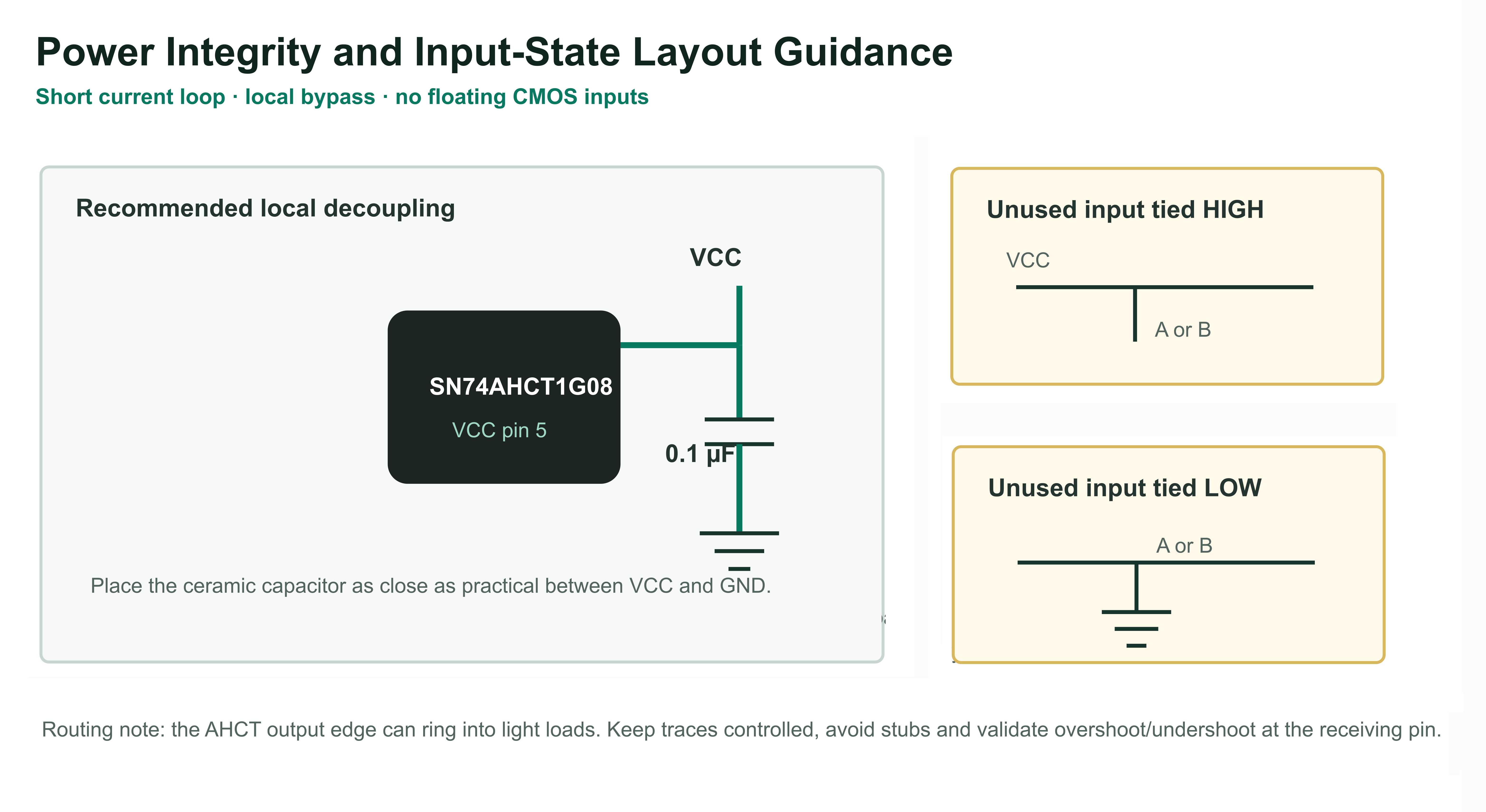
- Keep the supply loop short: route VCC, the bypass capacitor and GND with low inductance.
- Do not float A or B: connect unused inputs to VCC or GND.
- Avoid bus contention: this is a driven CMOS output, not an open-drain output.
- Control the output trace: fast edges into light loads can ring; minimize stubs and excessive trace length.
- Check receiving-pin limits: validate overshoot, undershoot, settling and noise margin at the actual receiver.
- Validate power sequencing: Ioff supports partial power down, but total system paths through other components remain external.
SOT23-5 and SC70-5 Package, Land Pattern and Tape-and-Reel Data
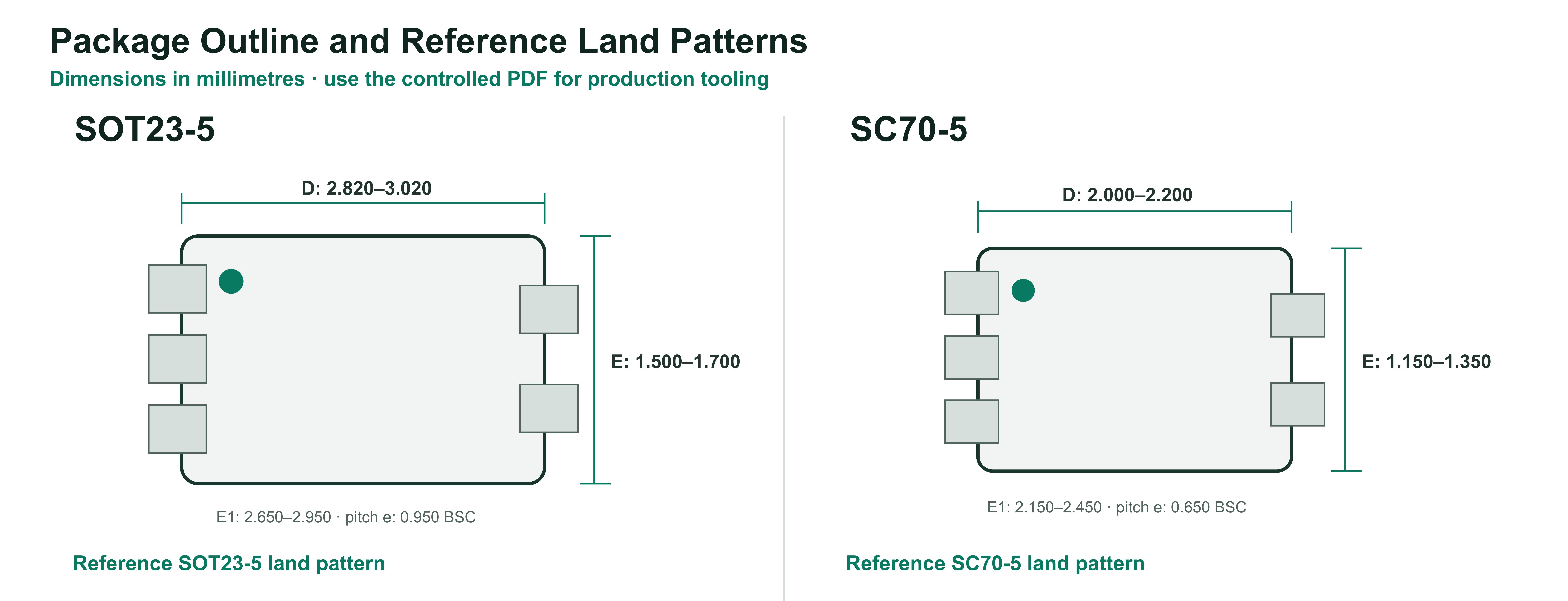
Package drawings and land patterns are displayed at high resolution for engineering review. PCB-library release must use the complete tolerance data in the controlled PDF and the assembler's process rules.
| Dimension | SOT23-5 minimum | SOT23-5 maximum | SC70-5 minimum | SC70-5 maximum | Unit |
|---|---|---|---|---|---|
| A, overall height | 1.050 | 1.250 | 0.900 | 1.100 | mm |
| A1 | 0.000 | 0.100 | 0.000 | 0.100 | mm |
| A2 | 1.050 | 1.150 | 0.900 | 1.000 | mm |
| b, lead width | 0.300 | 0.500 | 0.150 | 0.350 | mm |
| c, lead thickness | 0.100 | 0.200 | 0.080 | 0.150 | mm |
| D, body length | 2.820 | 3.020 | 2.000 | 2.200 | mm |
| E, body width | 1.500 | 1.700 | 1.150 | 1.350 | mm |
| E1, overall lead span | 2.650 | 2.950 | 2.150 | 2.450 | mm |
| e, nominal pitch | 0.950 BSC | 0.650 BSC | mm | ||
| L, lead length | 0.300 | 0.600 | 0.260 | 0.460 | mm |
| θ | 0° | 8° | 0° | 8° | degree |
| Package | Reel | Reel width | A0 | B0 | K0 | P0 / P1 / P2 | W | Pin 1 |
|---|---|---|---|---|---|---|---|---|
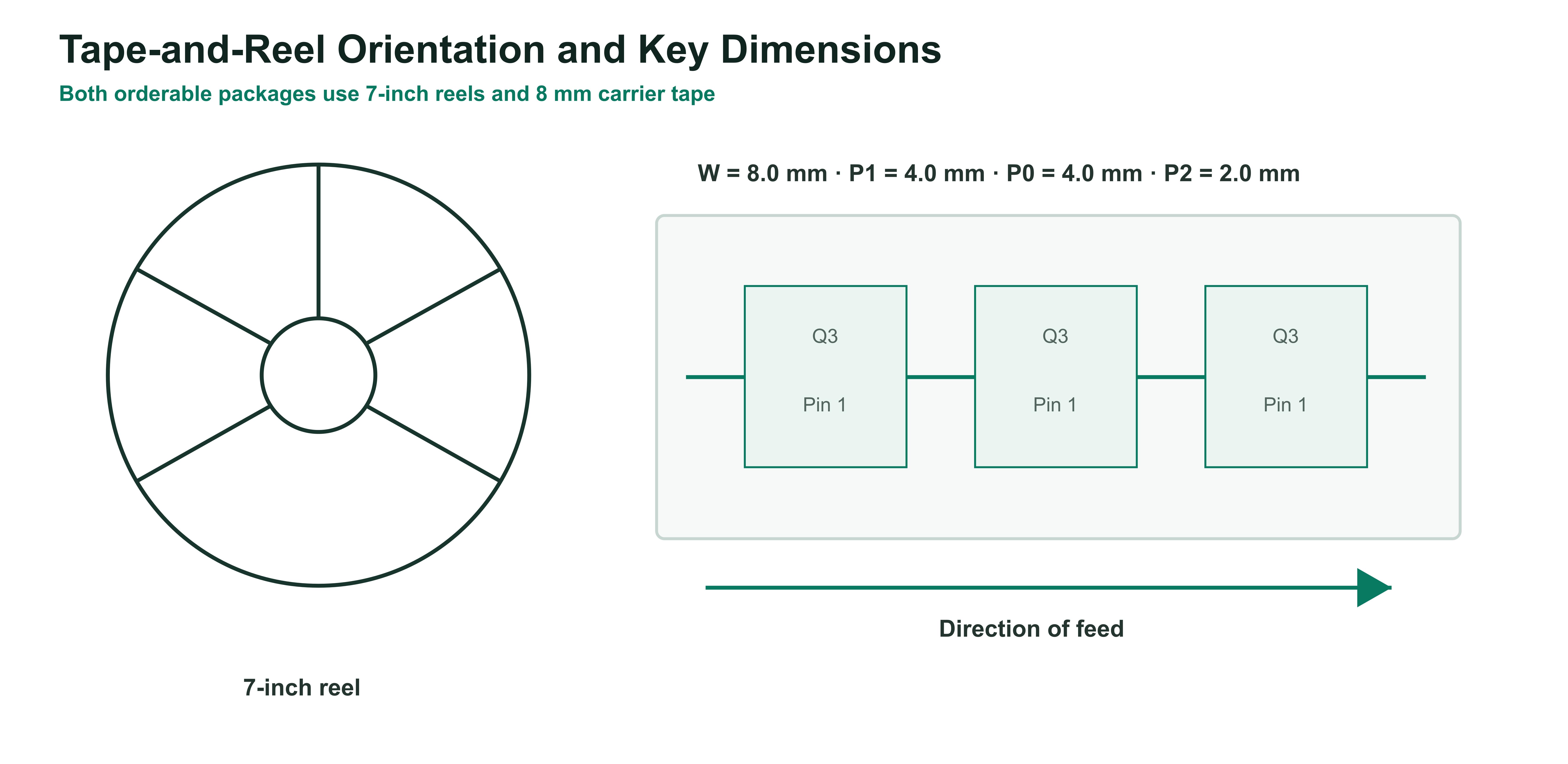
| SC70-5 | 7 in | 9.5 mm | 2.25 mm | 2.55 mm | 1.20 mm | 4.0 / 4.0 / 2.0 mm | 8.0 mm | Q3 |
| SOT23-5 | 7 in | 9.5 mm | 3.20 mm | 3.20 mm | 1.40 mm | 4.0 / 4.0 / 2.0 mm | 8.0 mm | Q3 |
Application Guidance and Design Limitations
The product specification lists active-noise elimination, bar-code scanners, blood-pressure monitors, CPAP machines, fingerprint identification and network-attached storage. The gate is also described for power sequencing and LED indicator logic. These are application examples—not end-product qualification statements.
 Power Sequencing and Logic EnableCombine two valid-state signals before enabling a downstream function. This gate does not generate sequencing delays.
 Status and LED GatingDrive a logic-qualified indicator when both input conditions are HIGH. Add a suitable current-limiting path.
 Portable Medical EquipmentExample categories include blood-pressure monitors and CPAP machines; system qualification remains mandatory.
 Barcode and Biometric ScannersQualify an acquisition or control signal from two logic conditions in barcode and fingerprint equipment.
 Network-Attached StorageUse for local enable, reset qualification or status logic after verifying system timing and voltage domains.
SN74AHCT1G08 Engineering FAQs
What logic function does SN74AHCT1G08 perform?
It performs one 2-input positive-AND function. Y is HIGH only when A and B are both HIGH; otherwise Y is LOW.
What supply-voltage range is specified?
The recommended operating VCC range is 2.0 V to 5.5 V. Absolute maximum VCC is 6.5 V, but the absolute maximum is a stress limit and is not an operating target.
Are the inputs TTL compatible?
The specification describes the inputs as TTL-voltage compatible. At VCC from 4.5 V to 5.5 V, VIH is 2.0 V minimum and VIL is 0.8 V maximum. Confirm the driving device's guaranteed levels and noise margin.
Can an input be left open?
No. Every unused input must be held at VCC or GND. A floating CMOS input can assume an undefined voltage, increase current and produce unpredictable output switching.
What does Ioff provide?
Ioff supports partial-power-down operation by limiting current when VCC is 0 V and an input or output is at 5.5 V. It helps prevent current backflow through the device output path, but does not validate the complete system power sequence.
Is 4.1 ns a guaranteed maximum propagation delay?
No. The 4.1 ns value is typical at VCC = 5.0 V ±0.5 V, CL = 50 pF and RL = 500 Ω. The AC table states that the values are ensured by design or characterization and are not production tested.
Which orderable package should be selected?
SN74AHCT1G08DCKR is the SC70-5 option with marking BEG. SN74AHCT1G08DBVR is the SOT23-5 option with marking B08S. Select by land pattern, assembly capability, body size and ordering code—not only by the shared base part number.
How should the device be decoupled?
Use a local bypass capacitor between VCC and GND. The product specification recommends 0.1 µF for a single-supply device, placed as close as practical to the power pins.
Can the output directly drive a high-current load?
The output drive data are logic-output specifications under defined voltage and current conditions, not a general load-power rating. Use a transistor or driver for relays, motors, high-power LEDs and other loads that exceed the DC, transient or thermal limits.
Does the application list establish product certification?
No. The listed application examples do not establish medical, automotive, safety or regulatory qualification. Qualification applies to the complete selected component revision and finished system.
This page summarizes SN74AHCT1G08_(RevA.1).pdf for component evaluation and engineering reference. It does not replace the complete controlled specification. Confirm the current revision, ordering code, package marking, pin assignment, logic thresholds, absolute maximum ratings, DC and AC conditions, load circuit, package tolerances, PCB layout, assembly process and qualification requirements before production release.
