

01 · Device purpose
Product Overview and Selection Scope
SN74LVC1G34 integrates one non-inverting buffer gate with a push-pull output.
- Wide supply range: operation from 1.65 V to 5.5 V.
- Non-inverting logic: Y follows A in positive logic.
- Input range up to 5.5 V: A is specified from 0 V to 5.5 V.
- Output drive: ±24 mA at VCC = 3.0 V under the specified DC test conditions.
- Low static supply current: 0.1 µA typical ICC at +25 °C.
- Partial-power-down support: Ioff limits current flow through the device when VCC = 0 V.
Selection boundary: This device is a single non-inverting push-pull buffer. It is not an inverter, open-drain output, three-state bus driver, dual-supply level translator, or analog switch.
02 · Logic and pins
Buffer Function, Truth Table and Pin Assignment
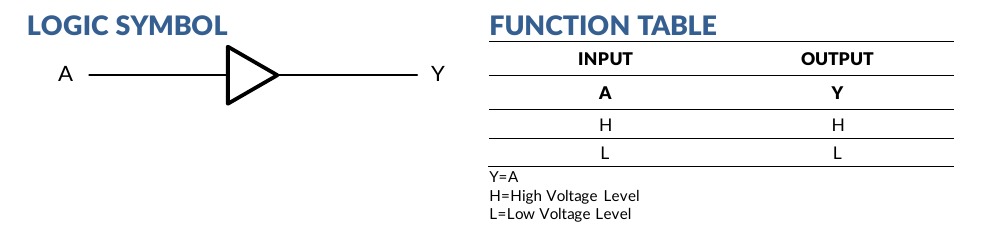
The output reproduces the input state: A LOW produces Y LOW, and A HIGH produces Y HIGH.
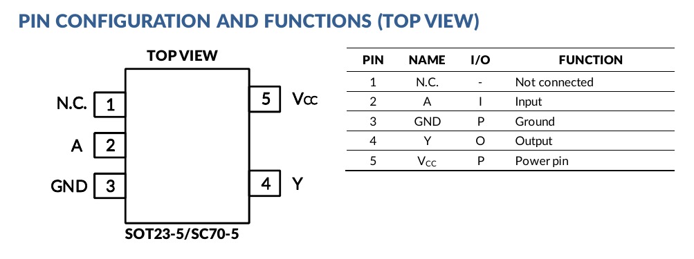
| Pin | Name | Type | Function | Engineering note |
|---|---|---|---|---|
| 1 | N.C. | - | Not connected | Leave electrically unconnected. |
| 2 | A | Input | Buffer input | Do not leave floating. |
| 3 | GND | Power | Ground | Use a short local return path. |
| 4 | Y | Output | Push-pull buffer output | Check output loading and receiver thresholds. |
| 5 | VCC | Power | Supply | Place local bypass capacitance close to pins 5 and 3. |
03 · Orderable options
Ordering Codes and Package Selection
| Ordering number | Temperature range | Package | Top marking | MSL | Packing |
|---|---|---|---|---|---|
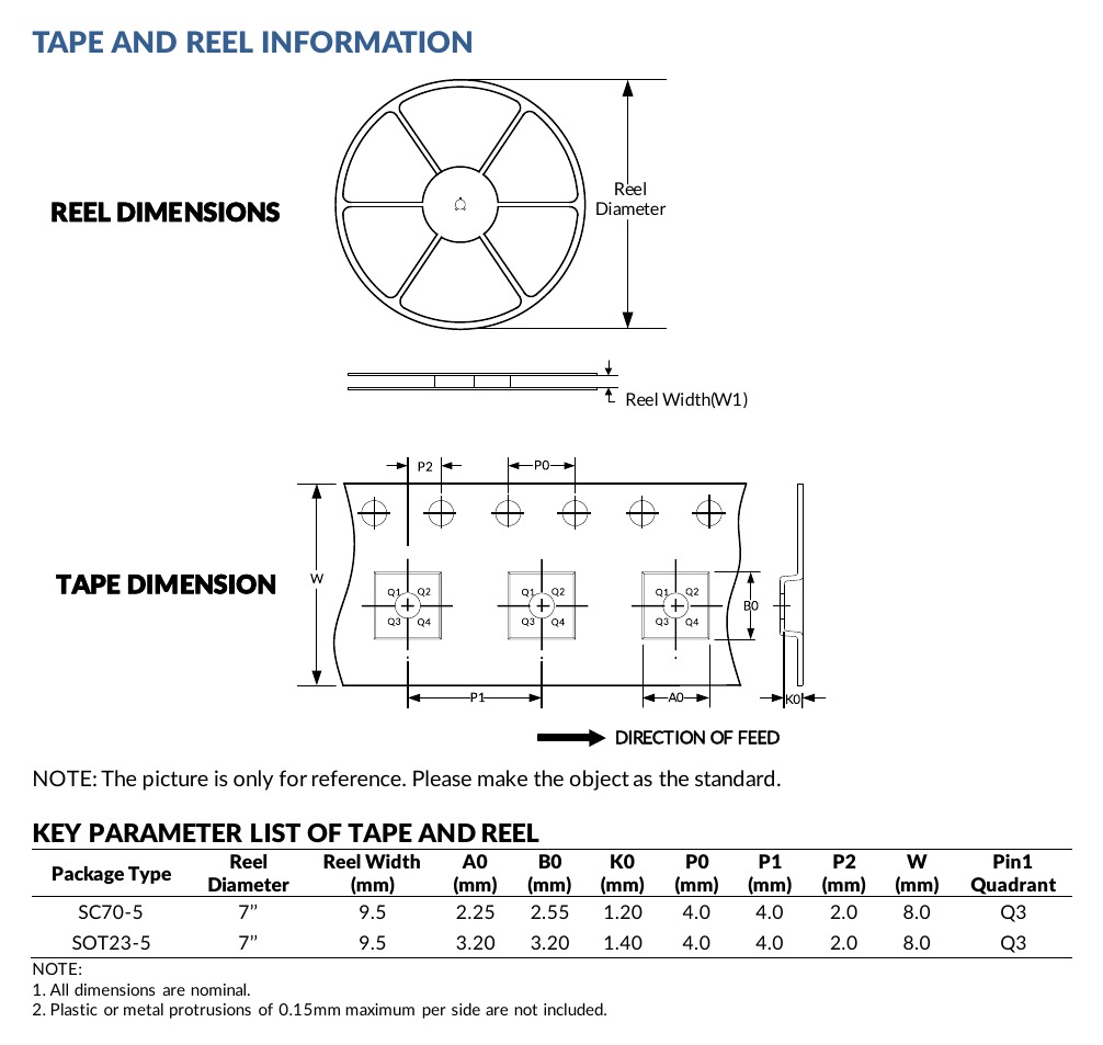
| SN74LVC1G34DCKR | -40 °C to +125 °C | SC70-5 / SOT353 equivalent | C95 | MSL 3 | Tape and reel, 3,000 units |
| SN74LVC1G34DBVR | -40 °C to +125 °C | SOT23-5 | C34J | MSL 3 | Tape and reel, 3,000 units |
Additional lot, date, vendor, logo or environmental markings may appear. Confirm the complete ordering code and package drawing during receiving inspection.
04 · Design envelope
Recommended Operating Conditions and Absolute Limits
| Parameter | Condition | Minimum | Maximum | Unit |
|---|---|---|---|---|
| Supply voltage, VCC | Operating | 1.65 | 5.5 | V |
| Supply voltage, VCC | Data retention only | 1.5 | Not specified | V |
| Input voltage, VI | Operating | 0 | 5.5 | V |
| Output voltage, VO | Operating | 0 | VCC | V |
| Input transition, Δt/Δv | 1.8 V / 2.5 V supplies | - | 20 | ns/V |
| Input transition, Δt/Δv | 3.3 V / 5.0 V supplies | - | 10 / 5 | ns/V |
| Ambient temperature, TA | Operating | -40 | 125 | °C |
Input logic thresholds
| VCC range | VIH minimum | VIL maximum | Unit |
|---|---|---|---|
| 1.65 V to 1.95 V | 0.65 × VCC | 0.35 × VCC | V |
| 2.3 V to 2.7 V | 1.7 | 0.7 | V |
| 3.0 V to 3.6 V | 2.0 | 0.8 | V |
| 4.5 V to 5.5 V | 0.7 × VCC | 0.3 × VCC | V |
Absolute maximum and handling limits
| Parameter | Minimum | Maximum | Unit |
|---|---|---|---|
| Supply voltage, VCC | -0.5 | 6.5 | V |
| Input voltage, VI | -0.5 | 6.5 | V |
| Output voltage, high-impedance or power-off | -0.5 | 6.5 | V |
| Output voltage, HIGH or LOW state | -0.5 | VCC + 0.5 | V |
| Input / output clamp current | -50 when the associated pin voltage is below 0 V | mA | |
| Continuous output current | ±50 | mA | |
| Continuous VCC or GND current | ±100 | mA | |
| Maximum junction temperature | Not applicable | 150 | °C |
| Storage temperature | -65 | 150 | °C |
05 · Static performance
Output Levels, Leakage and Supply Current
| Parameter | Test condition | VCC | Limit or typical value | Unit |
|---|---|---|---|---|
| VOH | IOH = -100 µA | 1.65 V to 5.5 V | Minimum VCC - 0.1 V | V |
| VOH | IOH = -4 / -8 / -16 / -24 / -32 mA | 1.65 / 2.3 / 3.0 / 3.0 / 4.5 V | Minimum 1.2 / 1.9 / 2.4 / 2.3 / 3.8 V | V |
| VOL | IOL = 100 µA | 1.65 V to 5.5 V | Maximum 0.1 V | V |
| VOL | IOL = 4 / 8 / 16 / 24 / 32 mA | 1.65 / 2.3 / 3.0 / 3.0 / 4.5 V | Maximum 0.45 / 0.30 / 0.40 / 0.55 / 0.55 V | V |
| II | A at 5.5 V or GND | 0 V to 5.5 V | ±0.1 µA typical; ±5 µA maximum full range | µA |
| Ioff | VI or VO = 5.5 V | 0 V | ±0.1 µA typical; ±10 µA maximum full range | µA |
| ICC | VI = 5.5 V or GND, IO = 0 | 1.65 V to 5.5 V | 0.1 µA typical; 10 µA maximum full range | µA |
| ΔICC | One input at VCC - 0.6 V | 3 V to 5.5 V | 500 µA maximum | µA |
| Ci | VI = VCC or GND | 3.3 V | 4 pF typical | pF |
06 · Dynamic performance
Propagation Delay and Dynamic Capacitance
| Parameter | 1.8 V | 2.5 V | 3.3 V | 5.0 V | Condition / unit |
|---|---|---|---|---|---|
| Propagation delay, tpd | 13.2 | 5.2 | 4.0 | 3.5 | Typical ns; CL = 30 pF or 50 pF |
| Power-dissipation capacitance, Cpd | 16 | 18 | 18 | 20 | Typical pF at 10 MHz |
Timing interpretation: The listed propagation delays are typical characterization values, not guaranteed worst-case limits. Validate the receiver threshold, PCB capacitance, supply tolerance, and operating-temperature range.
07 · Implementation
Input Control, Output Loading and PCB Guidance
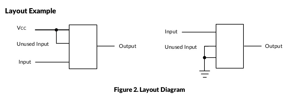
- Do not leave A floating: drive the input from a defined logic source or hold it at VCC or GND when unused.
- Leave N.C. open: pin 1 is not connected internally and should not be used as a routing tie point.
- Observe transition-rate limits: keep input rise and fall rates within the specified ns/V limits for the selected supply.
- Avoid output contention: Y actively drives HIGH and LOW; do not connect competing push-pull outputs.
- Budget fan-out: check VOH, VOL, output current and cumulative receiver capacitance.
- Bypass locally: place a 0.1 µF capacitor close to VCC and GND; the PDF also notes that 0.1 µF and 1 µF capacitors are commonly paralleled.
System check: Validate input thresholds, input transition rate, propagation delay, output loading, power sequencing, ESD protection, and signal integrity across the full production operating range.
08 · Mechanical
SOT23-5 and SC70-5 Packages, Land Patterns and Packing
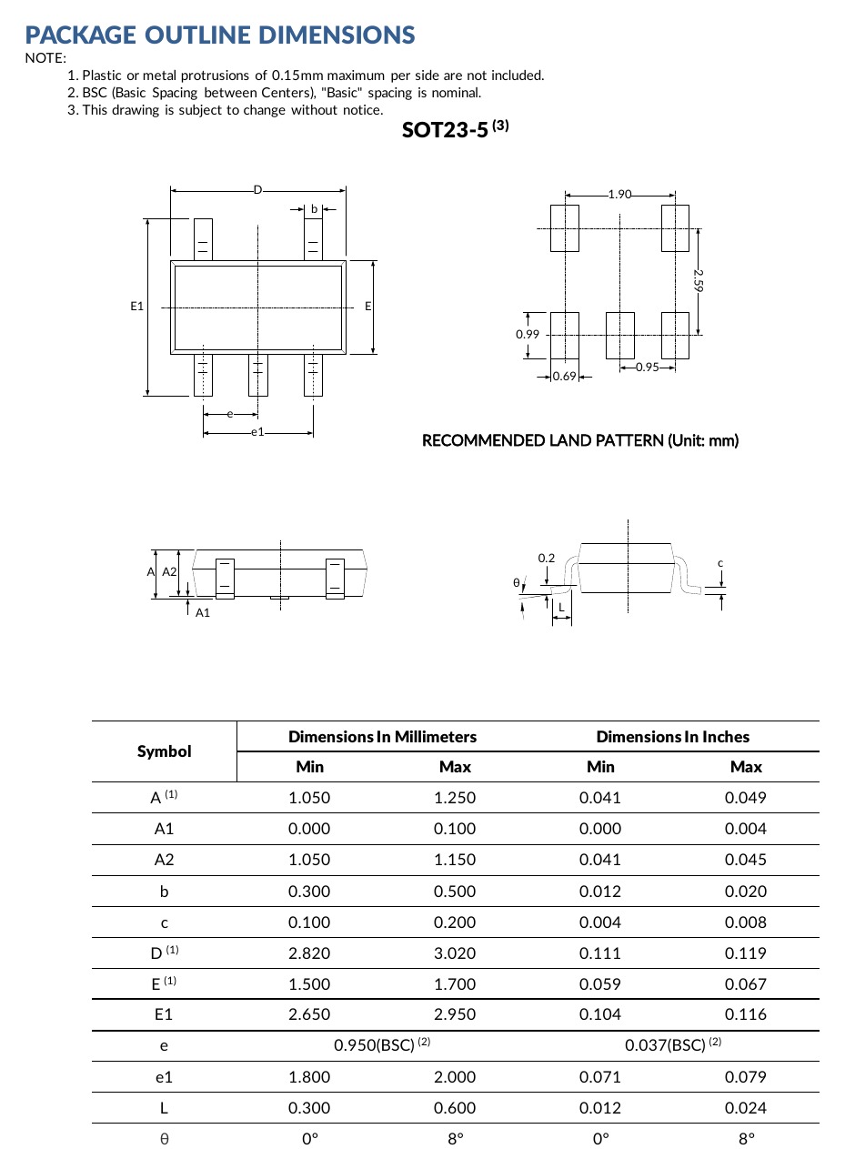
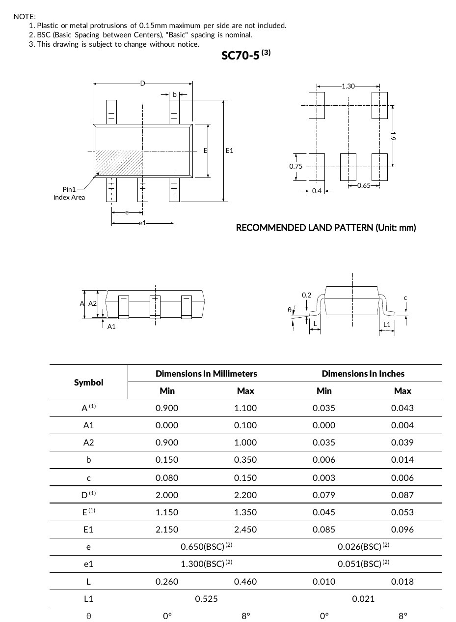
The two packages share the same logical pin assignment but have different body dimensions, lead pitch, marking and thermal impedance. Do not share one PCB footprint between them.
| Dimension | SOT23-5 | SC70-5 | Unit |
|---|---|---|---|
| Overall height A | 1.050 to 1.250 | 0.900 to 1.100 | mm |
| Body length D | 2.820 to 3.020 | 2.000 to 2.200 | mm |
| Body width E | 1.500 to 1.700 | 1.150 to 1.350 | mm |
| Overall lead span E1 | 2.650 to 2.950 | 2.150 to 2.450 | mm |
| Lead pitch e | 0.950 BSC | 0.650 BSC | mm |
| Outer lead pitch e1 | 1.800 to 2.000 | 1.300 BSC | mm |
| Lead width b | 0.300 to 0.500 | 0.150 to 0.350 | mm |
| Lead length L | 0.300 to 0.600 | 0.260 to 0.460 | mm |
09 · Use contexts
Application Guidance and Design Limitations
The supplied specification lists the following application areas. These are use contexts, not end-product approvals or safety certifications.
 AV ReceiversBuffer control and status signals after threshold and timing validation.
 Blu-ray and Home TheaterRestore logic drive across compact audio-video control paths.
 Desktop and Notebook PCsIsolate and strengthen board-level control signals.
 Digital Video CamerasBuffer logic between low-voltage control domains.
 Mobile PhonesProvide compact single-channel signal buffering.
 GPS NavigationStrengthen digital control signals in portable navigation equipment.
 Portable Media PlayersBuffer low-voltage control paths in battery-powered media hardware.
10 · Engineering answers
SN74LVC1G34 Engineering FAQs
What function does SN74LVC1G34 implement?
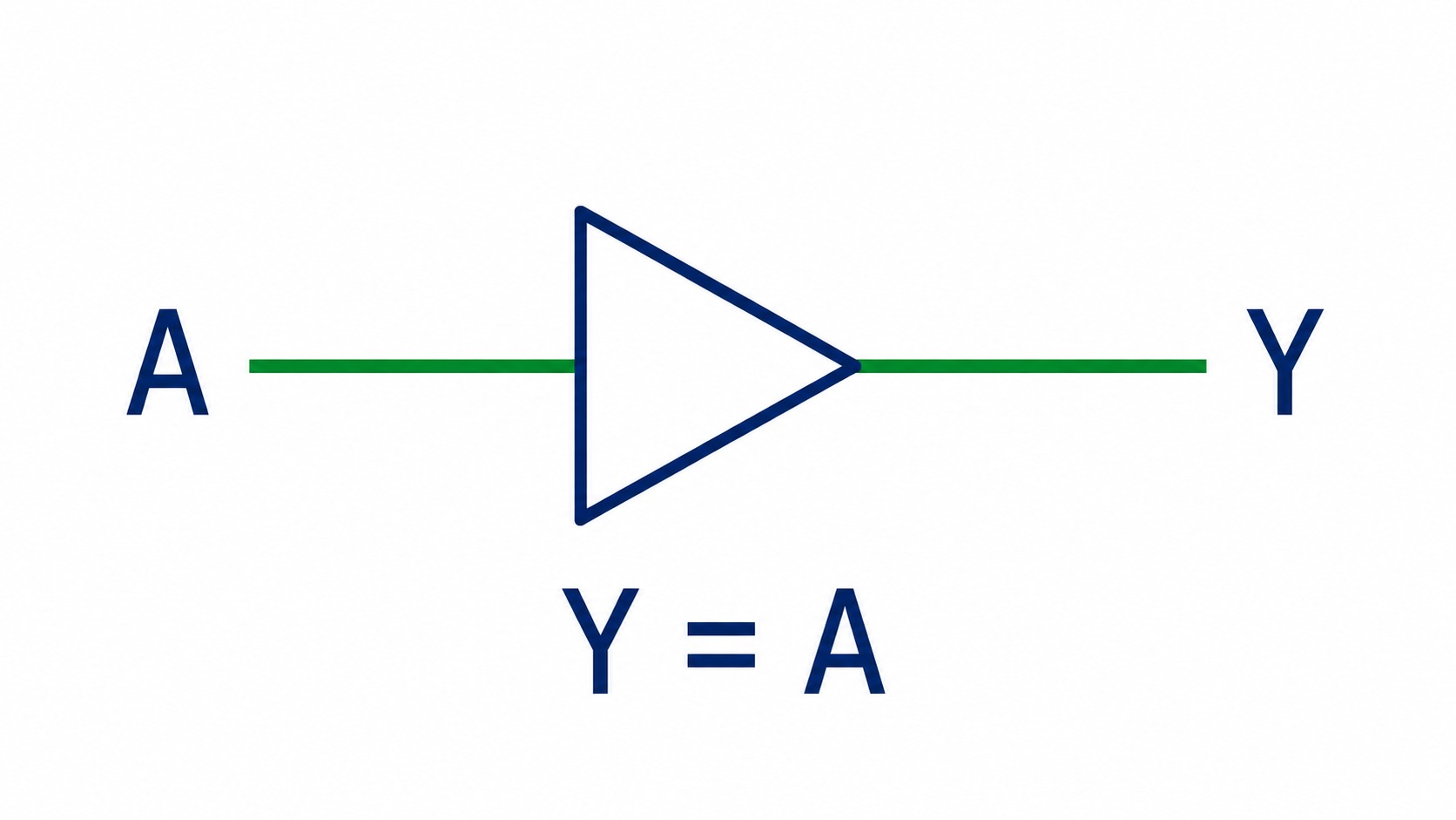
It performs Y = A. The output follows the input without inversion.
Is this an inverter?
No. A LOW produces Y LOW, while A HIGH produces Y HIGH.
What supply range is recommended?
VCC is specified from 1.65 V to 5.5 V for operation.
Can the input accept 5.5 V when VCC is lower or off?
The recommended input range is 0 V to 5.5 V, and Ioff is specified for partial power-down. Validate all board-level back-power paths.
What is the propagation delay?
The PDF lists typical propagation delays of 13.2 ns at 1.8 V, 5.2 ns at 2.5 V, 4.0 ns at 3.3 V, and 3.5 ns at 5.0 V under the stated load conditions. The specification does not provide guaranteed maximum propagation-delay limits.
Can the output be wire-connected with another output?
No. Y is a push-pull output. Do not connect it directly against another actively driven output.
Which packages are listed?
SN74LVC1G34DBVR is SOT23-5 with C34J marking. SN74LVC1G34DCKR is SC70-5 with C95 marking. Both are MSL 3 and tape-and-reel packed in quantities of 3,000.
What should be done with pin 1?
Pin 1 is N.C. and should be left electrically unconnected. Input A on pin 2 must not float.
This page summarizes the supplied SN74LVC1G34 Rev A.1 product specification for component evaluation. Confirm the current controlled specification, ordering code, marking, pin assignment, electrical limits, package tolerances and qualification requirements before production release.
