
NF522 13.56 MHz Multi-Protocol RFID Reader IC
NF522 is a highly integrated 13.56 MHz RFID reader/writer IC intended for embedded contactless reader designs. It supports the ISO/IEC 14443 Type A, ISO/IEC 14443 Type B, and ISO/IEC 15693 protocols, enabling data read and write operations with compatible contactless cards or tags. The device provides SPI, I²C, and UART host interfaces and integrates a 64-byte transmit/receive FIFO, configurable CRC-16 generation and verification, a programmable timer, interrupt control, and low-power card detection.
Product scope:NF522 is a reader/writer IC rather than a complete card reader module incorporating a PCB antenna and the required external components. Protocol support indicates only the communication protocols and reader/writer modes supported by the IC. The device itself does not provide NFC card emulation, peer-to-peer communication, application-layer security, or industry-specific certification..
The technical data includes register descriptions, interface timing, a typical application circuit, electrical characteristics, and package information. Use the current controlled document for design decisions.
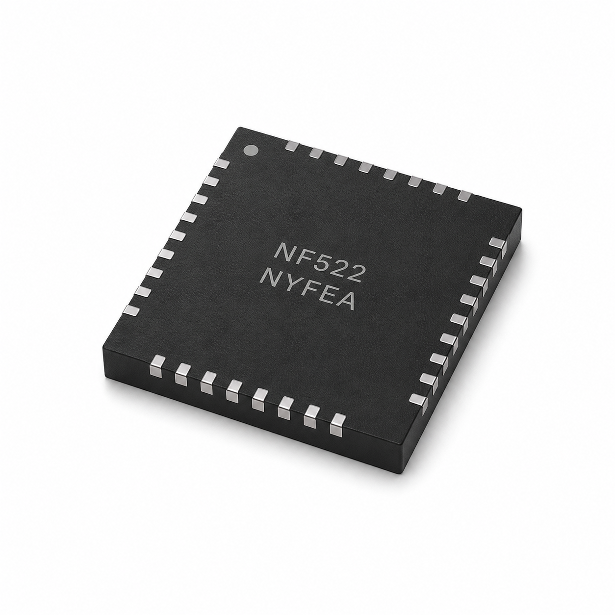
Product Overview
NF522 is designed for low-voltage, low-power, multi-protocol 13.56 MHz contactless readers. It handles RF transmission and reception, data buffering, CRC generation/checking, timing, and interrupt control. An external MCU configures the device and runs the reader sequence through the selected host interface.
NF522 supports reader modes for ISO/IEC 14443 Type A, ISO/IEC 14443 Type B, and ISO/IEC 15693. A system designer must still evaluate the target cards or tags, antenna, matching network, firmware, security architecture, regulatory requirements, and final enclosure.
Key Features
- Multi-protocol reader: ISO/IEC 14443 Type A, Type B, and ISO/IEC 15693 reader modes.
- High data rates: Type A and Type B support 106, 212, 424, and 848 kbit/s.
- ISO/IEC 15693: Single-subcarrier and dual-subcarrier modes.
- Host connectivity: SPI, I²C, and UART selected through interface configuration pins.
- Low-power operation: Hard Power-Down, Soft Power-Down, and low-power card detection (LPCD).
- Data buffering: 64 Byte transmit/receive FIFO.
- Data integrity: Configurable CRC16 generation and checking.
- Timing and control: Programmable timer and configurable interrupt output.
- Clocking: On-chip oscillator circuit for an external 27.12 MHz crystal.
- Separated supply domains: Independent host-interface and RF-transmitter supply domains.
- Reader distance: Data-sheet statement of up to 100 mm, dependent on antenna design and system conditions.
- M1 mode: The data sheet lists an M1 cryptographic mode; applicable card families, licensing, and security requirements must be confirmed for each project.
Protocols and Data Rates
ISO/IEC 14443 Type A
Supports 106, 212, 424, and 848 kbit/s.
ISO/IEC 14443 Type B
Supports 106, 212, 424, and 848 kbit/s.
ISO/IEC 15693
Single-subcarrier operation up to 52.97 kbit/s and dual-subcarrier operation up to 26.69 kbit/s.
These values describe IC capability. The usable protocol, data rate, and stable reading distance also depend on the card or tag, RF link, antenna matching, host firmware, and system timing.
Host Interfaces
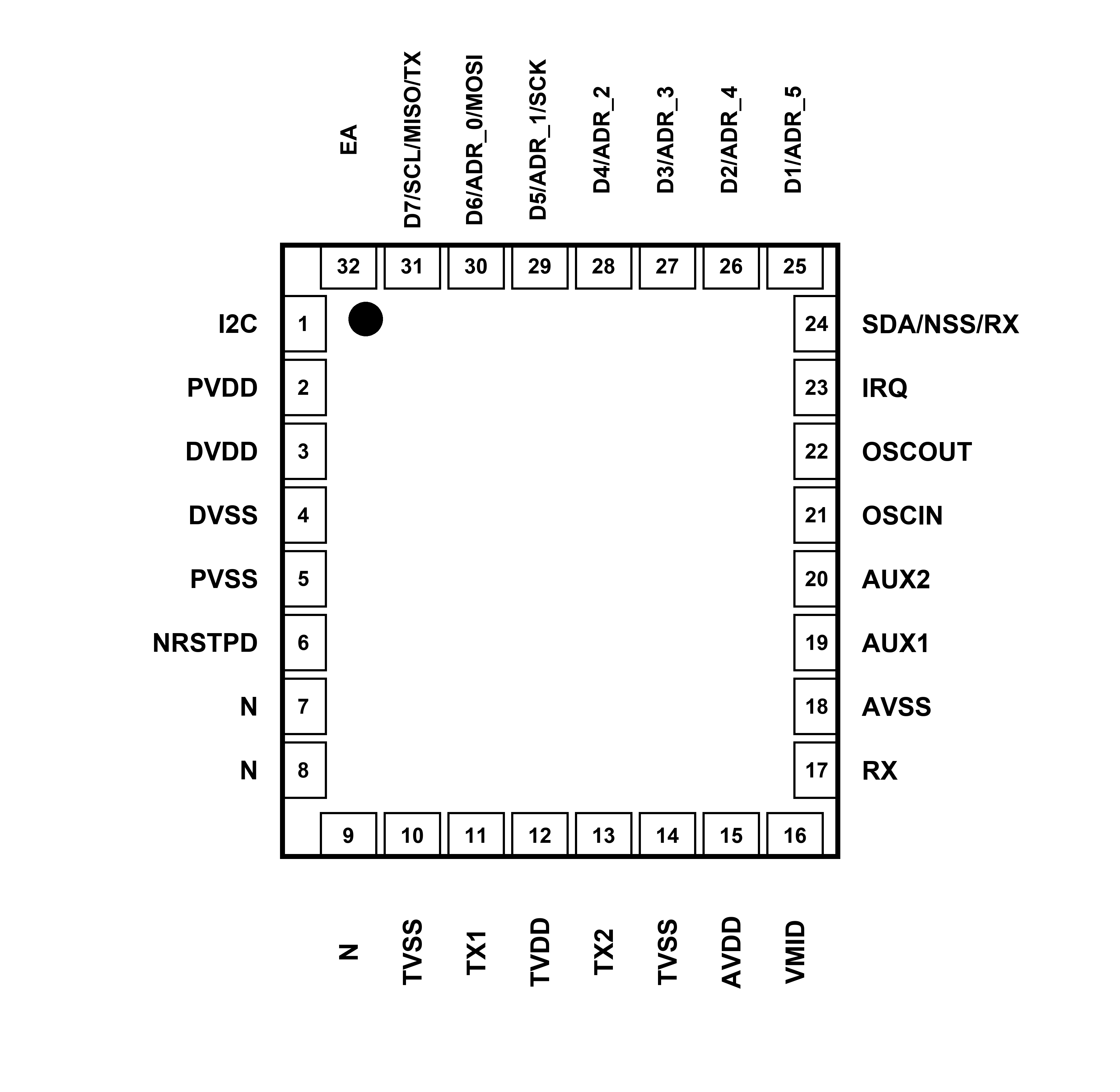
NF522 detects the selected host-interface configuration after power-on reset using the EA, I2C, and associated multiplexed pins. The schematic must be checked against the current pin-definition table for the selected interface.
| Interface | Role or format | Maximum data rate | Design notes |
|---|---|---|---|
| SPI | Slave; modes 0 and 3 | 12 Mbit/s | NSS, SCK, MOSI, and MISO use multiplexed pins. |
| I²C | 7-bit device address | 400 kbit/s | The hardware address is sampled and locked after reset release. |
| UART | 8 data bits, 1 stop bit, no parity, LSB first | 1.2288 Mbit/s | The RS-232 reference concerns serial framing, not RS-232 electrical levels. Use a level translator for a true RS-232 port. |
Low-Power Modes
| Mode | Disabled or retained functions | Exit or wake-up | System use |
|---|---|---|---|
| Hard Power-Down | Digital supply, analog supply, crystal oscillator, and internal RC oscillator are disabled. I/O is isolated; registers and FIFO contents are lost. | Release NRSTPD high; the IC restarts and must be initialized. | Lowest specified IC static state when full reinitialization is acceptable. |
| Soft Power-Down | The oscillator is disabled; I/O state, registers, FIFO contents, and configuration are retained. | Clear the PowerDown bit. With an external crystal, wait for oscillator stabilization. | Retains configuration and reduces the restart sequence. |
| LPCD | I/O state, registers, FIFO contents, and configuration are retained while low-power card detection operates. | A detected card or the wake timer exits LPCD; related status can be reported through IRQ. | Standby card detection for battery-powered or duty-cycled readers. |
Electrical Operating Conditions
| Symbol | Parameter | Minimum | Typical | Maximum | Unit |
|---|---|---|---|---|---|
| Tamb | Ambient operating temperature | -25 | +25 | +85 | °C |
| TVDD | Transmitter supply | 2.0 | 3.3 | 5.0 | V |
| PVDD | Pin/host-interface supply | 2.0 | 3.3 | 5.0 | V |
| AVDD | Analog supply | 2.3 | 3.3 | 5.0 | V |
| DVDD | Digital supply | 2.3 | 3.3 | 5.0 | V |
Typical current values listed in the technical data
| Supply or symbol | Condition | Typical value | Unit |
|---|---|---|---|
| IDVDD | Powered, before RF carrier transmission | 4.94 | mA |
| IDVDD | CW = 2, RF carrier transmitted | 6.97 | mA |
| IDVDD | Soft Power-Down | 263 | µA |
| IDVDD | Hard Power-Down | 0 | µA |
| IAVDD | Powered, before RF carrier transmission | 4.08 | mA |
| IAVDD | CW = 2, RF carrier transmitted | 4.11 | mA |
| IAVDD | Soft Power-Down | 1 | nA |
| IAVDD | Hard Power-Down | 0 | µA |
| TVDD supply current | TX1/TX2 open, TX1EN/TX2EN = 1, CW = 1 | 3.9 | mA |
| TVDD supply current | TX1/TX2 open, TX1EN/TX2EN = 1, CW = 2 | 4.34 | mA |
| TVDD supply current | TX1/TX2 open, TX1EN/TX2EN = 0 | 0 | µA |
| ILPCD | AVDD = TVDD = 3.3 V, external clock | 9.27 | µA |
Currents from different supply domains must not be added or interpreted without considering the actual power architecture and operating state. Measure complete-system current with the final MCU, regulator, RF settings, antenna, and peripherals.
RF and Antenna Design
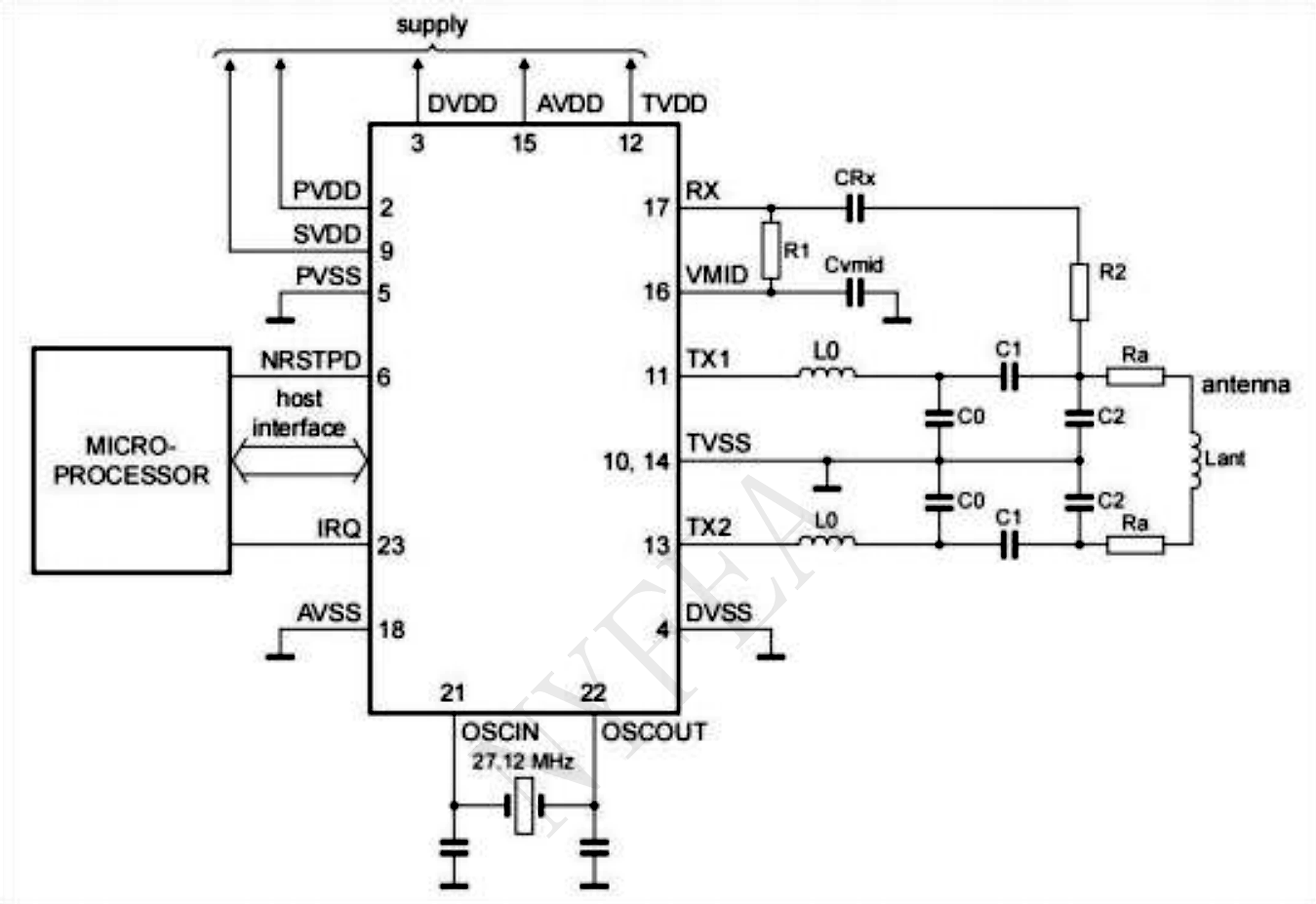
NF522 provides two 13.56 MHz transmitter outputs, TX1 and TX2, and an RX input. The typical application section states that one TX output may be left unconnected in a single-antenna design and recommends adjusting the antenna impedance to approximately 40–50 Ω.
The data sheet states a reader operating distance of up to 100 mm and explicitly qualifies it as dependent on antenna design. Actual reading distance is a system result determined by the IC, card or tag, antenna geometry and Q factor, matching network, supply voltage, PCB layout, enclosure material, nearby metal, communication rate, and firmware settings.
Typical Application Circuit
The typical circuit includes the host MCU interface, IRQ, reset/power-down control, a 27.12 MHz crystal, separated supply domains, RX/VMID receive circuitry, TX1/TX2 transmitter paths, and the external antenna matching network. The diagram below preserves the original wiring, pin numbers, component references, text, and layout of Figure 6-1 in the NF522 technical data; only deterministic upscaling, background cleanup, contrast adjustment, and sharpening have been applied.
Product Appearance and QFN32 Package
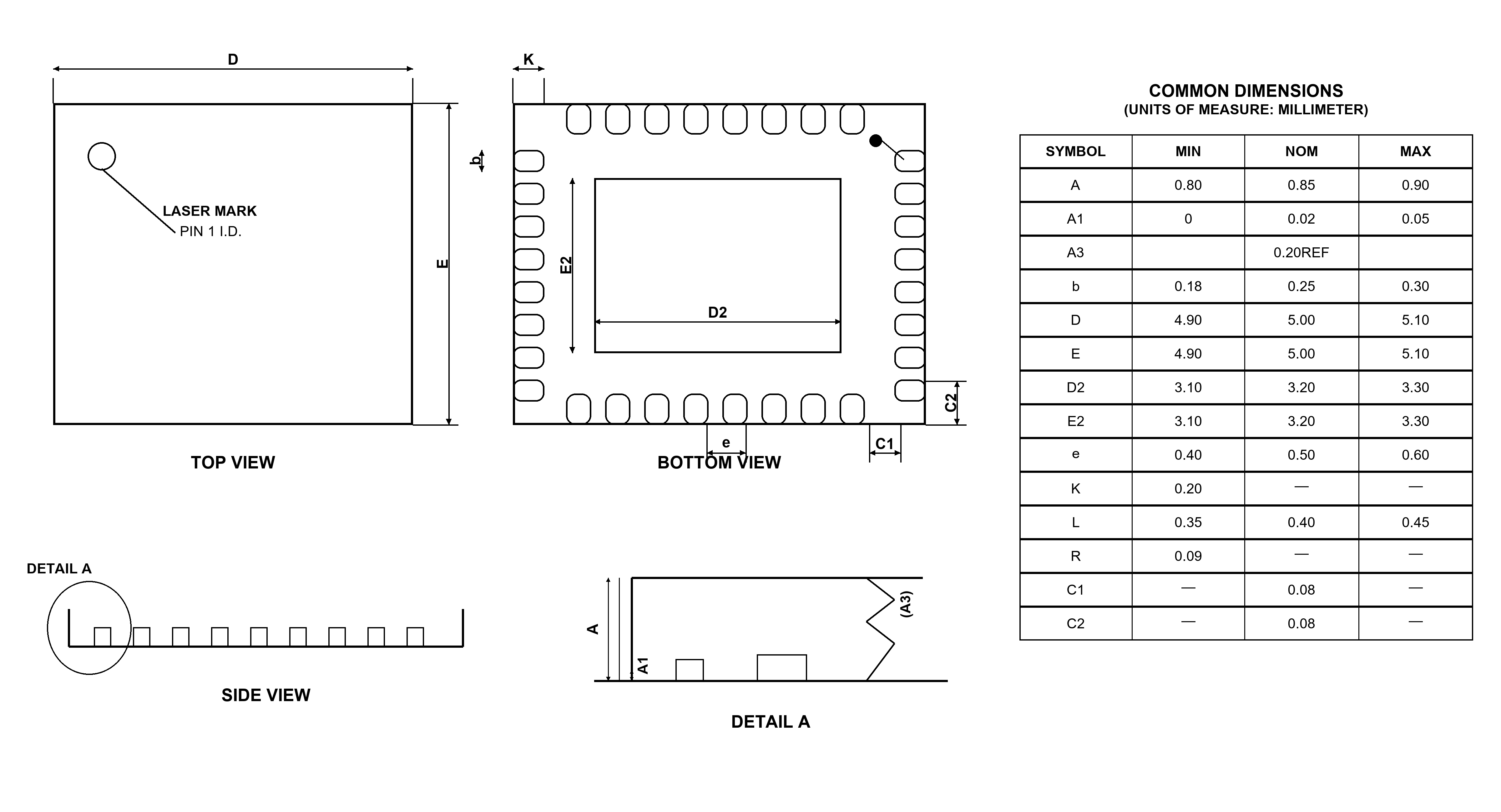
NF522 is supplied in a QFN32 package. The package appearance illustration is for webpage presentation only. Device identification, PCB land pattern, stencil, reflow process, and mechanical dimensions must be based on the current controlled technical data and physical device markings.
| Item | Specification | Design note |
|---|---|---|
| Package | QFN32 | Create and review the PCB land pattern from the current package drawing. |
| External clock | 27.12 MHz crystal | Connect to OSCIN/OSCOUT; also review the external clock-input option in the data sheet. |
| Reset and power-down | NRSTPD | Combined reset and Hard Power-Down control input. |
| Interrupt | IRQ | Configurable interrupt output; LPCD-related status can be routed to IRQ. |
| FIFO | 64 Byte | Transmit and receive data buffer. |
- Confirm the target card or tag protocol, data rate, security, and certification requirements.
- Select SPI, I²C, or UART and verify EA, I2C, and all multiplexed pin connections.
- Review TVDD, PVDD, AVDD, and DVDD supply domains and host MCU I/O levels separately.
- Complete the schematic and PCB using the controlled QFN32 package, reset, and clock information.
- Test initialization, polling, anti-collision, authentication, read/write operations, interrupts, and fault recovery.
- Validate RF performance, current consumption, temperature, EMC, and production variation in the final mechanical assembly.
Product Application Areas
These categories describe potential uses based on the available protocols, interfaces, and low-power features. The application pages are not yet available, so the categories are intentionally non-clickable.
 IndustrialEquipment identification, tool or consumable authentication, and parameter configuration.
 Communications Equipment, Computers, and PeripheralsPeripheral pairing, near-field configuration, accessory identification, and device identification.
 Automotive and In-Vehicle TerminalsEvaluation only; component qualification, reliability evidence, traceability, and end-product validation are required.
 IoT ApplicationsDevice onboarding, identification, parameter writing, and low-power wake-up.
 Personal ElectronicsSmart locks, portable readers, accessory identification, and device setup.
Engineering FAQs
What is an RFID reader IC?
An RFID reader IC is the semiconductor device that implements the radio-frequency transmit, receive, and digital reader functions needed to communicate with compatible RFID tags or contactless cards. NF522 is a 13.56 MHz multi-protocol RFID reader IC supporting ISO/IEC 14443 Type A, ISO/IEC 14443 Type B, and ISO/IEC 15693 in reader mode; it is one component of a complete reader, not a finished reader.
What does an RFID reader chip do?
An RFID reader chip generates and modulates the RF field, sends commands, receives and demodulates tag responses, and transfers data and status to a host processor. In NF522, supporting functions include a 64-byte FIFO, CRC16, programmable timers, interrupt signaling, and SPI, I²C, or UART host interfaces. The MCU, antenna, matching network, power, clock, firmware, and system validation remain part of the complete design.
RFID reader IC vs RFID module: what is the difference?
An RFID reader IC is the semiconductor component. An RFID reader module is a board-level assembly that normally combines a reader IC with some or all of the antenna or antenna connector, matching network, clock, power components, host connector, and sometimes an MCU and firmware. NF522 belongs to the IC category, so a complete reader based on NF522 requires external hardware, firmware, RF tuning, and product-level validation.
NFC reader IC vs NFC controller: what is the difference?
The terms are not used consistently across all suppliers. Reader IC usually emphasizes the RF field and tag or card reader function, while NFC controller often implies additional protocol or control integration and may support broader NFC operating modes. Compare the specified standards, modes, interfaces, software stack, and qualifications rather than relying on the product name. NF522 is specified as a 13.56 MHz RFID reader IC for ISO/IEC 14443 Type A, ISO/IEC 14443 Type B, and ISO/IEC 15693 reader modes; this page does not claim NFC Forum controller certification, peer-to-peer mode, or card-emulation mode.
Which RFID reader IC should I choose?
Start with the operating frequency and the standards used by the target tags or cards. Then compare reader modes and data rates, host interfaces, power modes, RF output and antenna-matching requirements, package and temperature range, software support, qualification evidence, and supply requirements. NF522 is a candidate for 13.56 MHz embedded readers that need ISO/IEC 14443 Type A, Type B, or ISO/IEC 15693 with SPI, I²C, or UART; it is not a UHF reader IC. Prototype testing with the final antenna, enclosure, and target tags is required.
Which RFID and NFC standards does NF522 support?
NF522 supports ISO/IEC 14443 Type A, ISO/IEC 14443 Type B, and ISO/IEC 15693 in reader mode. Type A and Type B support 106, 212, 424, and 848 kbit/s.
Which host interfaces and data rates does NF522 support?
NF522 supports SPI, I²C, and UART. SPI operates as a slave at up to 12 Mbit/s, I²C supports up to 400 kbit/s, and the UART baud-rate table extends to 1.2288 Mbit/s.
What is the typical NF522 current in low-power card detection mode?
The data sheet specifies a typical LPCD current of 9.27 µA with AVDD = TVDD = 3.3 V and an external clock. This is an IC-level value under the stated conditions, not the standby current of a complete reader.
What read range can NF522 achieve?
The data sheet states a reader operating distance of up to 100 mm and explicitly notes that it depends on antenna design. Actual range also depends on the card or tag, antenna geometry, matching network, supply conditions, PCB layout, enclosure, nearby metal, and firmware settings.
Can NF522 directly replace MFRC522?
NF522 should not be described as a drop-in, pin-to-pin, register-level, or firmware-compatible replacement for MFRC522 unless this is proven for the specific design. It can be evaluated as an alternative for a new or redesigned 13.56 MHz reader, but migration must compare supported tag technologies, footprint and pins, power rails, host-interface behavior, register map, firmware, antenna matching, EMC, and target-tag performance. Complete validation is required before production.
Can the NF522 UART connect directly to RS-232 voltage levels?
No such direct electrical compatibility should be assumed. The data sheet reference to RS-232 concerns serial framing; the NF522 interface must be designed to the IC electrical limits, with an appropriate level translator when connecting to a true RS-232 port.
Is NF522 specified as an automotive-grade IC?
The available NF522 technical data does not state AEC-Q100 or equivalent automotive qualification. Automotive or in-vehicle use requires supplier qualification evidence, traceability, reliability assessment, and project-level validation.
