CLRC663 Antenna Design and Read Range Guide: NF663 Evaluation
A practical engineering guide to CLRC663 antenna geometry, impedance matching, VNA measurements, enclosure effects, limited read-range diagnosis and controlled NF663 evaluation.
DIRECT ANSWER
CLRC663 read range is not a fixed IC specification. It is a system-level result determined by the complete 13.56 MHz RF path: antenna geometry, losses and quality factor (Q), the EMC and matching networks, transmitter and receiver configuration, card size and orientation, supply integrity, enclosure materials, nearby metal, firmware timing, and the test acceptance criteria.
When evaluating NF663 for a new or redesigned reader, do not assume that the original CLRC663 antenna network remains valid. First establish a reproducible CLRC663 baseline, then test the NF663 prototype with the same cards, fixtures, enclosure configurations and acceptance criteria.
Scope and Evidence Boundaries
Search queries often use the family-level term “CLRC663.” Engineering records must identify the full order code, silicon variant, data-sheet revision, board revision and firmware version.
Report read range, impedance, current, temperature, LPCD behavior and enclosure performance only for a clearly defined board and test setup.
Functional overlap between CLRC663 and NF663 does not prove pin, register, firmware, electrical or RF-network compatibility.
Why CLRC663 Has No Single Read-Range Number
A search for “CLRC663 read range” often implies that one distance in centimeters should describe the IC. That number has little engineering value unless the card, antenna, protocol, supply, enclosure and acceptance rule are stated at the same time.
The same reader PCB can behave differently with a full-size ISO/IEC 14443A card, a small key fob and an ISO/IEC 15693 label. A bare board can also lose range after installation beside a battery or metal mounting plate. A single successful transaction at the maximum observed distance is not equivalent to a range that a production reader can support repeatedly.
A card is detected at least once under favorable positioning and timing. This is useful during exploration, but not as a release criterion.
The reader repeatedly completes the required protocol exchange at a defined position and orientation.
Multiple boards, device samples, cards and assembly states meet a documented acceptance criterion across the specified temperature range.
IC, development-board and module data are not interchangeable
Search results often combine IC data sheets, official development kits, third-party modules and finished readers, even though their range figures are not interchangeable. An IC data sheet characterizes the device under defined electrical conditions. A module claim also reflects that module’s PCB antenna, matching components, power supply, firmware and selected card. It cannot be converted into a universal CLRC663 specification or used to predict the performance of an NF663 board with a different RF network.
Define the Test Baseline Before Changing the Antenna
A common debugging mistake is to change the matching capacitors, card, test distance, firmware and enclosure at the same time. Performance may improve, but the cause remains unknown. Freeze the baseline, then change one controlled variable at a time.
| Item | Record | Why it matters |
|---|---|---|
| Reader device | Full order code, top mark, package and data-sheet revision | Variants within the same family may have different electrical requirements. |
| Protocol | ISO/IEC 14443A/B, ISO/IEC 15693 or other required mode | Protocol, data rate and card technology affect the RF test. |
| Cards / tags | Chip, form factor, antenna size and sample IDs | A large card and a small key fob do not present the same coupling conditions. |
| Antenna | Outline, turns, trace width/spacing, inductance, loss and board stack | This establishes the physical RF baseline. |
| Power | Voltage, ripple, current limit and operating load | The transmitter is part of the power system, not an isolated load. |
| Assembly | Bare PCB, ferrite, battery, metal, cover and final installation | The environment can detune and damp the antenna. |
| Card position | Center, edge, corner, offset, tilt and approach motion | Center-only testing overstates the usable interaction area. |
| Pass rule | Attempts, allowed retries, success rate and time limit | Without one rule, two range results cannot be compared. |
For example, a project might define a fixed card position and run 100 transactions at each distance boundary. The sample count and success threshold are project-specific; both must be defined before hardware is compared.
Read Range Belongs to the Complete RF Signal Chain
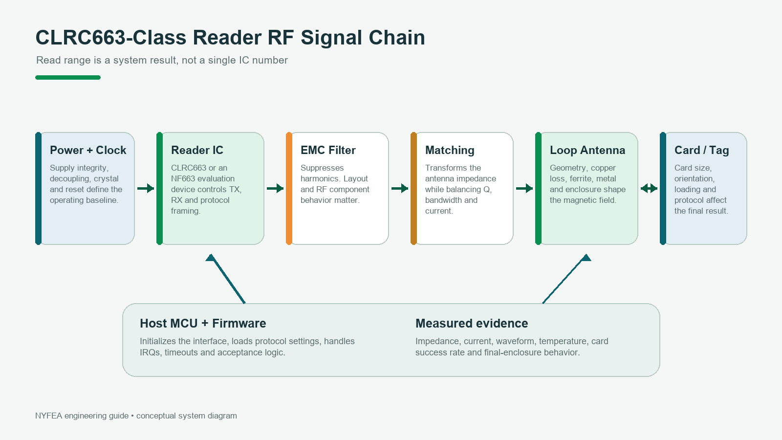
The reader IC is one block in a larger system. The transmit and receive paths are related, but they are not a single one-way chain:
Transmit: power and clock → reader IC → TX outputs → EMC filter → matching network → loop antenna ⇄ card. Receive: card load modulation → loop antenna → receiver coupling and bias network → RXP/RXN → reader IC → host MCU and firmware.
A fault in any block can appear as “short range” or intermittent card detection. Confirm the host interface, reset sequence, oscillator, protocol configuration and RF-field activation before treating the failure as an antenna problem.
CLRC663 Antenna Geometry: What the Drawing Actually Controls
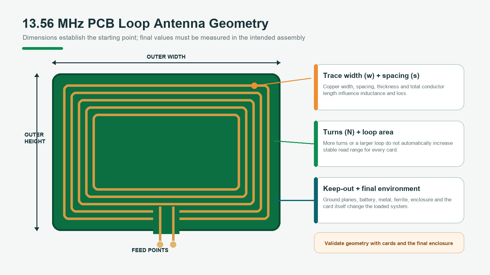
A PCB loop is not designed by drawing a 13.56 MHz rectangle and selecting a generic capacitor. Outer dimensions, turn count, trace width, spacing, copper thickness, via placement and feed routing contribute to inductance, series loss, parasitic capacitance, Q factor and field distribution.
Loop size must follow the target cards and tags
A larger reader loop is not automatically better for every small tag. More turns also do not guarantee more stable range. Geometry must be chosen around the actual card set, available product area, expected presentation zone and nearby materials.
Q is a tradeoff, not a score
Insufficient Q can reduce the available field strength and degrade receiver performance. Excessive Q can narrow the bandwidth and make the assembly overly sensitive to component tolerances, card loading and environmental changes. The appropriate target balances field strength, bandwidth, current, protocol requirements and compliance.
RF components are not ideal
Matching capacitors and EMC inductors introduce tolerance, temperature coefficient, equivalent series resistance (ESR) and, where applicable, saturation effects. Prototype success with hand-selected components does not prove that the released BOM will perform the same way. Validate every supplier and tolerance range approved for production.
A card changes the loaded system
The no-card response is a baseline, not the final operating condition. A card couples to the magnetic field and loads the reader antenna. Its size, power demand, position and orientation can all change the response. A well-centered no-card S-parameter response does not prove reliable modulation, reception or protocol exchange with the card present.
Use VNA and Powered Reader Evidence Correctly
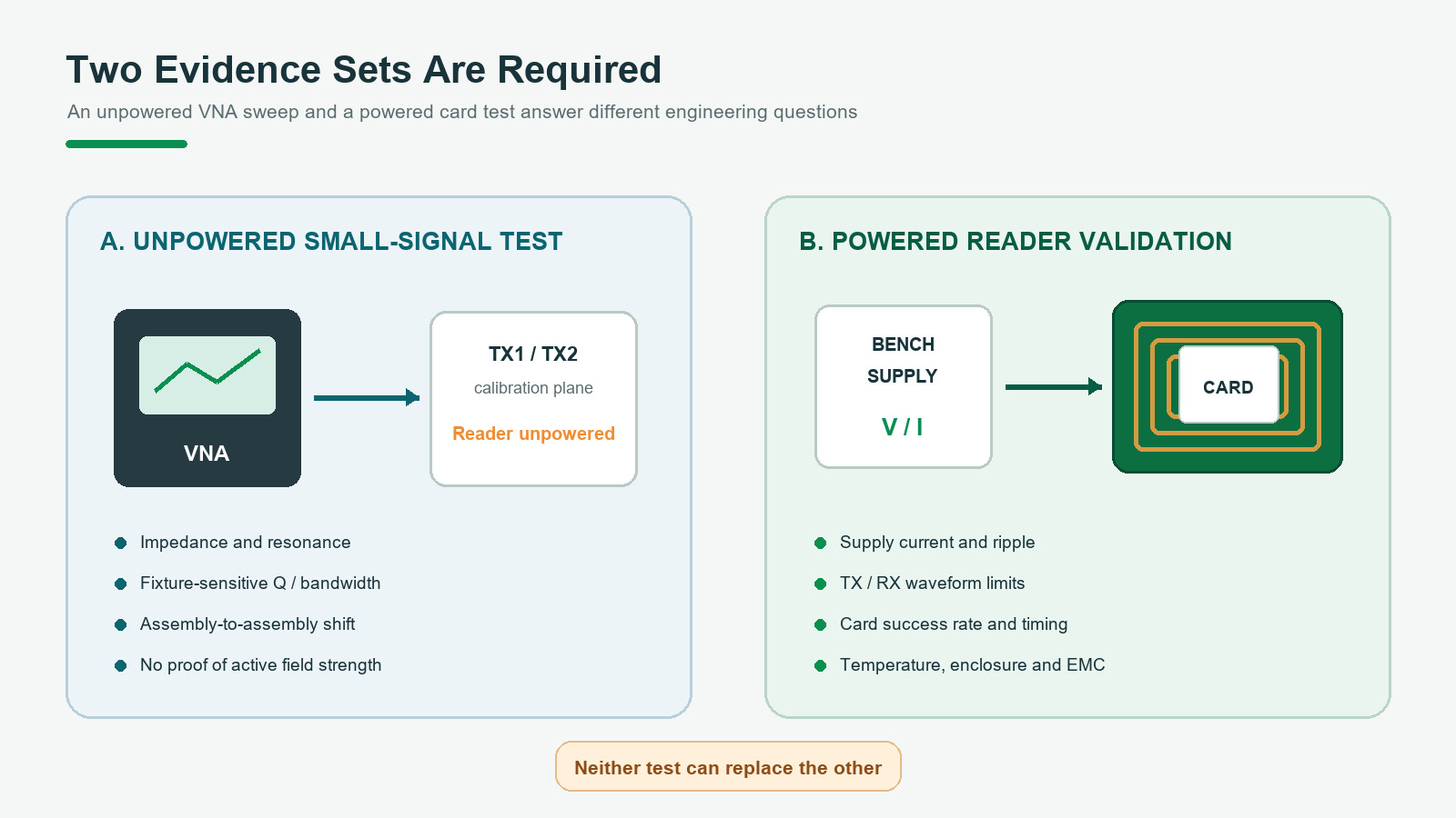
A vector network analyzer can reveal impedance and resonance changes, but the fixture is part of the measurement. Probes, cables, adapters and long temporary wires introduce their own parasitics. Calibrate as close as practical to the intended TX test points and document the connection method.
NXP’s AN11019 describes an S11 measurement between TX1 and TX2 with the reader unpowered and the VNA source kept at a low level—0 dBm or less in the application-note example. The method provides a repeatable small-signal baseline, but it does not reproduce active-transmitter behavior, supply droop, nonlinear effects, receiver limits or an actual card transaction.
Recommended design and tuning sequence
- Freeze the baseline. Archive the schematic, PCB revision, BOM, original matching values, firmware settings and test conditions.
- Define the requirements. Record the required protocols and data rates, target card matrix, acceptance range, supply limits, current boundary and EMC objectives.
- Calibrate the measurement setup. Calibrate the VNA, cable, probe and fixture at the defined measurement plane before measuring the antenna.
- Characterize the antenna coil. Measure inductance and series resistance at 13.56 MHz, and record the geometry and intended mechanical environment.
- Set the electrical targets. Define the target impedance and Q for the exact reader variant, required data rates, current limit and EMC constraints.
- Design the network. Define or verify the EMC filter, then calculate and simulate the matching network using the measured antenna values.
- Assemble, measure and correlate. Measure the complete unpowered network between TX1 and TX2, adapt the model and change one deliberate component group at a time.
- Validate the powered reader. Check supply integrity, transmitter current and waveforms, receiver-input behavior, component temperature and device limits.
- Run functional and enclosure tests. Execute real transactions with the target card matrix, then repeat the measurements with the final enclosure and nearby system electronics active.
- Confirm production margins. Test multiple PCBs and IC samples across released component suppliers, tolerances, supply and temperature limits, and applicable EMC conditions.
Small-signal and powered tests answer different questions
Maintain two evidence sets. The unpowered record should include the calibration method, measurement plane, sweep conditions, impedance, resonance, Q and assembly-to-assembly variation. The powered record should include supply voltage and ripple, transmitter current, relevant TX/RX waveforms, temperature, transaction timing and success rate.
CLRC663 uses a differential RF interface. A single-ended 50 Ω analyzer port does not mean the reader antenna should be connected as a universal 50 Ω load. The target presented to the driver depends on the exact device, supply, differential matching topology, desired field, current boundary and EMC design.
Why Read Range Changes After Installation
A bare board that performs well on a laboratory bench can lose range inside a smart lock, access reader or industrial terminal. The final assembly changes both distance and the electromagnetic environment.
Metal and batteries
Nearby conductors can develop eddy currents that add loss and reshape the magnetic field. A battery, metal backplate or lock body can also shift the antenna’s effective parameters. Even small mechanical changes may require RF revalidation.
Ferrite is a design change
Ferrite can help control the field near metal, but it also changes inductance and loss. After adding ferrite, remeasure the antenna and check current, temperature and card performance. Material grade, thickness, air gaps and production tolerance belong in the controlled BOM.
Display, main board and harness activity
Ground planes, displays, motors, switching supplies and digital harnesses can introduce loss or noise. A reader tested with the rest of the system disabled may not represent normal operation.
Cover thickness and user motion
The cover adds physical separation, while coatings, decorative metal and adhesive layers can add electromagnetic effects. Users do not hold every credential at the center, parallel to the loop and motionless. Test offset, tilt and approach speed.
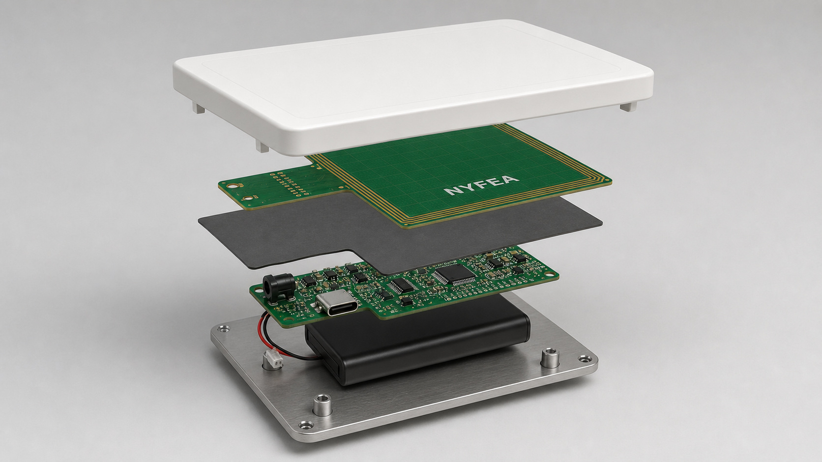
Use a progressive assembly sequence: bare PCB → battery → ferrite → main board and harness → complete enclosure → installed product. The first stage that produces a measurable change in the RF response identifies where further investigation should focus.
Do Not Optimize Range Past EMC, Current or Thermal Boundaries
More field is not automatically a better design. The output network also suppresses harmonics, and PCB layout influences filter performance. Changes made to increase range can raise transmitter current, component temperature, receiver input level or emissions.
NXP AN11019 treats antenna performance and CE/FCC compliance as part of the same matching problem. After any significant change to impedance, damping or transmitter configuration, recheck:
- voltage, peak demand and ripple on the relevant supply rails;
- transmitter-stage current against the exact device limit;
- TX and receiver-input behavior against electrical limits;
- temperature of the IC and RF components;
- fundamental field, harmonics and spurious emissions for the target market;
- performance and compliance across released component tolerances.
This guide does not state universal regulatory limits. Product category, antenna, measurement distance and destination market determine the applicable test program.
CLRC663 Short or Unstable Read Range: Troubleshooting Order
| Observed symptom | Check first | Controlled test |
|---|---|---|
| Bare-board range is good; range drops after assembly | Metal, battery, ferrite, cover and harness | Add one assembly layer at a time and remeasure. |
| Large cards work; small-tag range is limited | Coupling area and required card set | Fix the orientation and compare identified card and tag samples. |
| Center works; edge fails | Field distribution and usable presentation area | Measure a two-dimensional position grid. |
| Range changes between attempts | Power, EMI, card motion, timeout, excessive Q or detuning sensitivity | Use a fixture and log repeated transactions. |
| Boards differ significantly | Antenna build, RF component tolerance and assembly | Measure multiple boards and released suppliers. |
| One protocol is weaker | Protocol settings, bandwidth and target cards | Save configurations and results by protocol. |
| No card can be read at any distance | Power, reset, clock, interface, initialization and RF enable | Prove digital communication before retuning. |
A completely silent reader is not automatically an antenna failure. Verify power, reset, oscillator, SPI/I²C/UART communication, IRQ, register access, protocol loading and field activation first.
Communication Range and LPCD Detection Range Are Different Metrics
Normal card reading requires a completed protocol exchange. Low-Power Card Detection (LPCD) periodically samples the receiver response for a change, reducing the need for continuous active polling. Its engineering variables include the sleep interval, I/Q measurements, detection thresholds, wake timing, baseline drift and false-wake rate.
Calibrate the no-card I/Q baseline in the final mechanical and electrical configuration. Do not copy LPCD threshold values from another board, antenna or enclosure without repeating the calibration and validation.
Record at least:
- stable normal-mode communication range;
- reliable LPCD wake distance;
- false wake events with no card;
- missed detections with required cards;
- baseline behavior across temperature and assembly states;
- average current and wake response time.
A more sensitive threshold may improve detection but also increase false wakeups. Test LPCD in the final enclosure and operating environment. A successful LPCD wake does not prove that the subsequent card transaction will complete.
How to Evaluate NF663 Without Assuming CLRC663 Compatibility
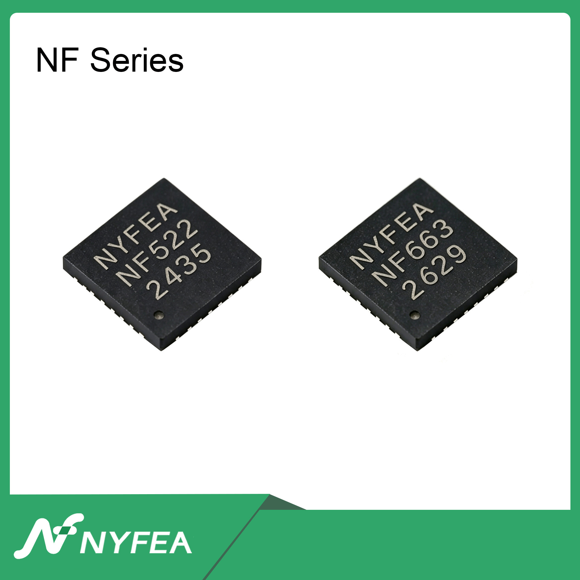
NF663 may be evaluated for a new multi-protocol 13.56 MHz reader or a controlled redesign. Similar supported functions do not establish compatibility. The project must review pins, exposed pad, supplies, interface selection, clock, reset, commands, registers, FIFO/EEPROM behavior, interrupts, RF network, package and production constraints.
Interpret the NF663 distance and impedance conditions correctly
The NF663 product specification supplied for this evaluation states a typical read/write operating distance of up to 12 cm with an ISO/IEC 14443A/MIFARE card, depending on antenna size and tuning. “Typical,” “up to” and “depending on antenna size and tuning” are essential conditions. The statement is not a guaranteed minimum and does not predict small tags, metal assemblies, other orientations, other protocols or every production unit.
For one typical TVDD-current entry, the same specification assumes a complementary driver and an antenna matched to 40 Ω between TX1 and TX2 at 13.56 MHz. That condition defines the table value; it is not a universal NF663 antenna-matching target and must not be copied into a CLRC663 design. Determine the required impedance and component values from the exact device documentation, the selected antenna and powered assembly tests.
A controlled five-gate evaluation
- Freeze the CLRC663 baseline: board, BOM, firmware, antenna, cards, enclosure states, power and acceptance rules.
- Audit the documents: compare exact pins, supplies, host-interface mode, package, commands, registers and RF network.
- Build dedicated NF663 hardware: include test points, current measurement and adjustable matching positions.
- Retune and validate: repeat unpowered RF, powered RF, card, enclosure, temperature, current and LPCD tests.
- Apply the production gate: approve only after multiple boards, devices, cards and boundary conditions pass.
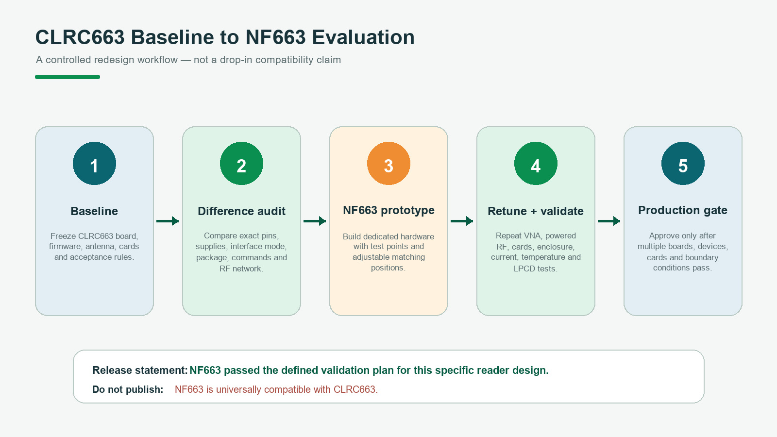
Use: “NF663 passed the defined validation plan for this specific reader design.”
Avoid: “NF663 is universally compatible with CLRC663.”
Production Acceptance Matrix
Record best-case performance, but qualify the product against the worst credible operating boundary. The matrix should expose variation and failure modes rather than reporting only an average.
| Dimension | Recommended coverage |
|---|---|
| Reader PCBs | Multiple boards and, where possible, manufacturing lots. |
| Reader devices | Multiple IC samples, not one hand-selected device. |
| Cards / tags | Required chip types, sizes, antenna forms and samples. |
| Protocols | Every mode released by the product. |
| Position | Center, edge, corner, offset, tilt and realistic presentation motion. |
| Supply | Allowed voltage range and representative system loads. |
| Mechanical state | Bare board, subassembly, complete cover and installed product. |
| Environment | Temperature, metal, ferrite and normal EMI-producing system states. |
| Transactions | Success rate, retry count, latency and classified errors. |
| LPCD | Wake distance, misses, false wakes, baseline drift and average current. |
| Extended operation | Repeated polling, thermal stability and recovery from faults. |
Conclusion
CLRC663 antenna design cannot be reduced to one read-range number, one resonance point or one matching value. A defensible result begins with a defined card set and pass rule, follows the complete RF chain, combines unpowered and powered evidence, and is repeated in the final mechanical environment.
If NF663 is being considered, treat it as an evaluation device for a new or redesigned reader. Preserve the CLRC663 baseline, audit every interface and RF boundary, build suitable prototype hardware, retune the network and release only against production-intent tests.
Frequently Asked Questions
What is the typical CLRC663 read range?
There is no useful universal distance without conditions. Antenna, matching, card, protocol, orientation, supply, enclosure, metal and the pass rule all affect the result. Treat external centimeter values as setup-specific until they are reproduced on production-intent hardware.
How should a CLRC663 antenna be tuned?
Freeze the hardware, cards, firmware, supply, fixture and enclosure state. Measure the antenna and matching network with a documented calibration plane, then correlate the result with powered current, waveforms and real card transactions. Change one deliberate variable at a time.
Is tuning to 13.56 MHz or 50 Ω enough?
No. 13.56 MHz is the carrier, while the useful matching target depends on the driver, differential network, supply, damping, bandwidth, current and EMC goals. A 50 Ω analyzer port is not proof that the reader antenna should be a direct 50 Ω load.
Why does CLRC663 range drop inside the enclosure?
Metal, battery, ferrite, display, ground planes, harnesses, coatings and physical spacing can detune or damp the loop. Add mechanical layers progressively, measure after each step and repeat the card matrix in the complete product.
Is LPCD range the same as normal communication range?
No. LPCD detects a change during a low-power sampling cycle; normal range requires a completed protocol exchange. Wake distance, false wakes, missed detections, average current and subsequent communication must be validated separately.
Can the CLRC663 antenna network be reused with NF663?
Do not assume it. The antenna geometry may be used as a comparison baseline, but the NF663 RF path, matching, current, receiver behavior, cards, enclosure and LPCD need to be remeasured on suitable hardware.
Is NF663 a drop-in replacement for CLRC663?
The available NF663 information does not establish universal pin, register, firmware, electrical or RF-network compatibility. Evaluate NF663 as a candidate for a new or controlled redesign and issue only a project-specific validation conclusion.
Primary Engineering Sources
- NXP — CLRC663 and CLRC663 plus Product Data Sheet
- NXP AN11019 — CLRC663, MFRC630, MFRC631, SLRC610 Antenna Design Guide
- NXP AN11145 — CLRC663 Low-Power Card Detection
- NYFEA — NF663 Multi-Protocol RFID Reader IC
- NYFEA NF663 Product Specification — consult NYFEA for the current controlled revision before using revision-sensitive values.
NEXT ENGINEERING STEP
Define the Baseline Before You Compare Reader ICs
Start with the exact card set, antenna, enclosure and production acceptance criteria. NYFEA can support an NF663 documentation review and controlled prototype evaluation without assuming direct CLRC663 compatibility.