CLRC66303HNY REPLACEMENT REVIEW · 13.56 MHz NFC/HF RFID
CLRC66303HNY Replacement: NF663 Pin, Firmware, PCB and RF Review
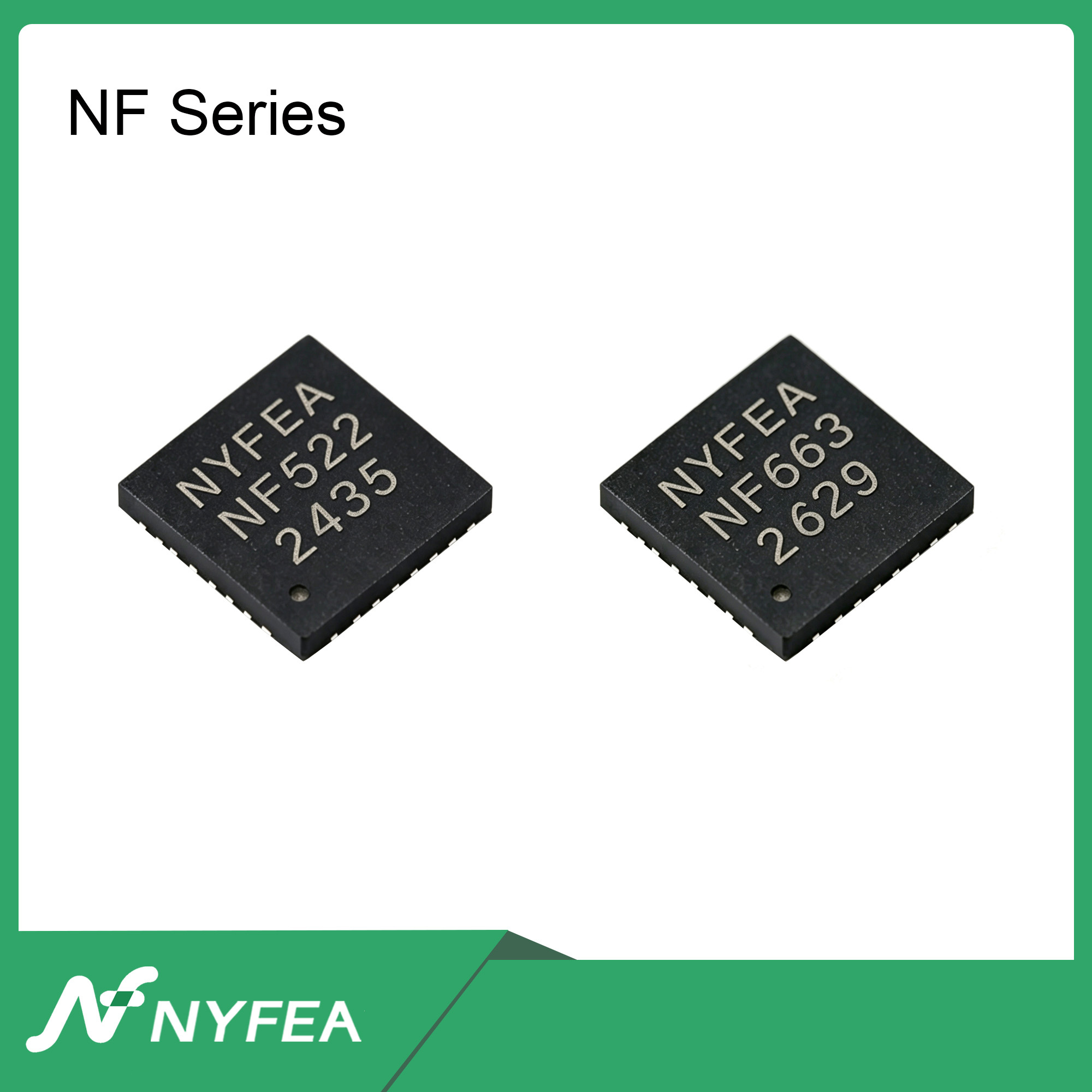
CLRC66303HNY is NXP's orderable wettable-flank HVQFN32 reel version of the CLRC663 plus multi-protocol NFC frontend. The published NF663 package and pin assignments align closely enough to support a controlled migration study, but they do not establish drop-in interchangeability. This guide defines the exact CLRC66303HNY baseline, the documented differences and the qualification work required before production release.
DIRECT ANSWER
NF663 can be evaluated as a CLRC66303HNY alternative when the package, pin mapping and product limits fit the application. The design must operate within the NF663 supply range of 3.0 V to 5.5 V and ambient range of −25 °C to +85 °C, and the firmware, RF network and finished product must be requalified before release.
What is CLRC66303HNY, and what does the HNY suffix mean?
CLRC66303HNY is the complete NXP ordering code for a CLRC663 plus multi-protocol NFC frontend in a wettable-flank HVQFN32 reel package. The suffix is important for procurement and qualification because a broad search for “CLRC663” can mix silicon revisions, package options, evaluation boards and third-party modules.
| CLRC66303HNY field | Documented value | Why it matters |
|---|---|---|
| Manufacturer and family | NXP Semiconductors, CLRC663 plus | Prevents comparison with earlier CLRC663 revisions or similarly named modules. |
| Orderable part number | CLRC66303HNY; NXP product identifier 935306208518 | Use the full MPN and identifier in AVL, BOM and incoming inspection records. |
| Function | Host-controlled 13.56 MHz multi-protocol NFC frontend | Defines the functional class an alternative must preserve. |
| Package | HVQFN32, SOT617-1, nominal 5 × 5 × 0.85 mm, wettable flanks | Wettable flanks support optical solder-joint inspection; compare the controlled land pattern and paste design. |
| Moisture and delivery | MSL2; HNY reel option with 6,000 devices | Controls storage, reflow handling and purchasing-unit assumptions. |
| Lifecycle check | NXP lists CLRC66303HNY as Active as checked September 13, 2026 | “Active” does not guarantee local stock, allocation status or future supply; verify the authorized channel at purchase time. |
| Operating baseline | 2.5 V to 5.5 V; −40 °C to +105 °C for CLRC66303; 13.56 MHz carrier | The supply and temperature limits are the first exclusion criteria when screening NF663. |
Can NF663 replace CLRC66303HNY?
Evaluate NF663 only if every selection gate below can be met.
Selection gates
- All reader supply rails remain within 3.0 V to 5.5 V.
- The required ambient range fits −25 °C to +85 °C.
- The team can review or port register-level firmware.
- The RF network and LPCD thresholds can be measured and retuned.
- Production-intent prototypes can complete the required qualification.
CLRC66303HNY vs NF663: what is documented and what requires validation?
Published data show close functional and pin-assignment alignment between CLRC66303HNY and NF663, but the specified operating limits are not identical. The table separates manufacturer-documented characteristics from items that require verification on the target hardware.
| Criterion | CLRC66303HNY | NF663 | Migration meaning |
|---|---|---|---|
| Product identity | NXP CLRC663 plus ordering code; HNY identifies the HVQFN32 reel option | NYFEA NF663 reader/writer IC | DOCUMENTED Treat the manufacturer, revision baseline and orderable part number as separate identity fields. |
| Carrier | 13.56 MHz | 13.56 MHz | OVERLAP A common carrier frequency does not make the RF networks interchangeable. |
| Reader protocols | ISO/IEC 14443 A/B, JIS X 6319-4, ISO/IEC 15693, ISO/IEC 18092 passive initiator, ICODE EPC and ISO/IEC 18000-3 mode 3 | ISO/IEC 14443 A/B, JIS X 6319-4, ISO/IEC 15693, ISO/IEC 18092 passive initiator, ICODE EPC and ISO/IEC 18000-3 mode 3 | OVERLAP Test the exact cards, commands, rates, security and anticollision cases. |
| Host interfaces | SPI up to 10 Mbit/s; I²C up to 1000 kBd; logic-level UART up to 1228.8 kBd | SPI up to 10 Mbit/s; I²C up to 1000 kBd; logic-level UART up to 1228.8 kBd | VALIDATE Equivalent interface names and rates do not establish identical startup, addressing, framing or timing. |
| FIFO and EEPROM | 512-byte FIFO; 8 kB EEPROM, including a documented 6 kB freely programmable area | 512-byte FIFO; 8 kB EEPROM organized as 64-byte pages | VALIDATE Similar capacity does not establish an identical memory organization or access model. |
| Timers and interrupt logic | Five timers and interrupt request registers | Five timer channels and two IRQ status/enable groups | VALIDATE Port host timeouts and interrupt handling against the NF663 register definitions. |
| Supply range | CLRC66303: 2.5 V to 5.5 V | NF663: 3.0 V to 5.5 V | DIFFERENT Any product that requires operation below 3.0 V falls outside the specified NF663 range. |
| Ambient temperature | −40 °C to +105 °C | −25 °C to +85 °C | DIFFERENT NF663 is unsuitable where the required ambient range extends below −25 °C or above +85 °C. |
| Package and pin assignment | HVQFN32, SOT617-1, nominal 5 × 5 × 0.85 mm, MSL2, wettable flanks | HVQFN32, SOT617-1, nominal 5 × 5 × 0.85 mm, MSL2 | PIN-ALIGNED The published tables map the same primary signal names to pins 1–32 and VSS to pad 33. Compare the controlled land patterns, solder-paste requirements, tolerances and electrical behavior. |
| LPCD | Supported; CLRC66303 adds flexible LPCD configuration | Supported with programmable I/Q thresholds | VALIDATE Measure sleep current, false wakes, missed cards and wake-to-transaction time. |
| Read-distance reference | Typical up to 12 cm for an ISO/IEC 14443 Type A/MIFARE card, depending on antenna size and tuning | Typical up to 12 cm for an ISO/IEC 14443 Type A/MIFARE card, depending on antenna size and tuning | VALIDATE Neither typical value guarantees read range in the finished product. |
| Drop-in compatibility | Package and pin-assignment alignment is documented; equivalent electrical, firmware, RF and production behavior is not. | VALIDATE Manage the change as a controlled redesign until every release criterion passes. | |
Evidence basis: The comparison uses NXP CLRC663 data sheet Rev. 5.4 and the cited NF663 product documents. “Documented” means that a value appears in a manufacturer source; “validate” means that target-hardware testing is still required.
Are NF663 and CLRC66303HNY pin-compatible?
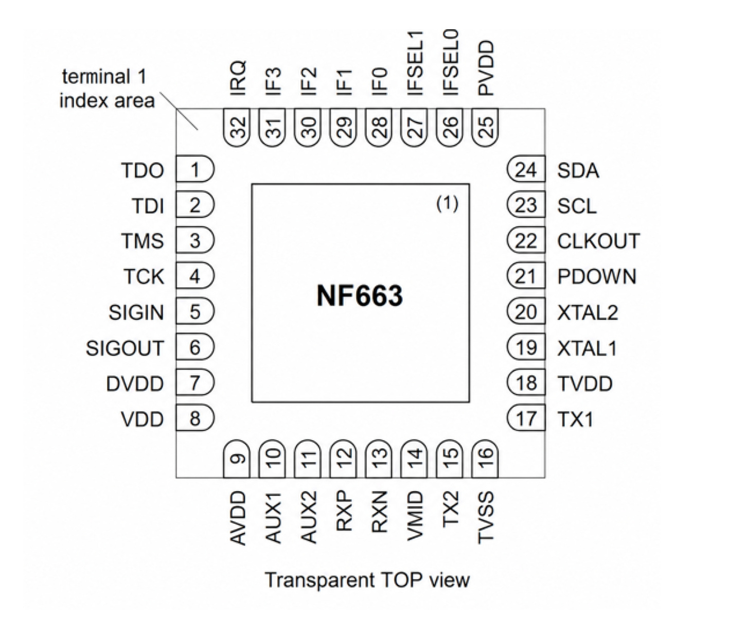
The published pin tables assign matching signal names to pins 1 through 32 and VSS to exposed pad 33. Use the grouped comparison for schematic review, then check each multifunction pin, I/O voltage and reset state against the controlled specifications.
| Pins | Published assignment in both devices | Migration check |
|---|---|---|
| 1–4 | TDO, TDI, TMS, TCK | Primary boundary-scan signals align. Verify boundary-scan enable state and any GPIO use at reset. |
| 5–6 | SIGIN, SIGOUT | Contactless/active-antenna signal positions align. Validate direction, pad configuration and timing if used. |
| 7–9 | DVDD, VDD, AVDD | Supply and regulator-buffer positions align. DVDD and AVDD are capacitor connections, not external supply inputs; compare capacitor and startup requirements. |
| 10–14 | AUX1, AUX2, RXP, RXN, VMID | Analog test/SAM and balanced receive-path positions align. Recheck loading, biasing and receive-network values. |
| 15–18 | TX2, TVSS, TX1, TVDD | Balanced transmitter positions align. Confirm TVDD operating conditions, transmitter current, EMC filter and antenna matching. |
| 19–22 | XTAL1, XTAL2, PDOWN, CLKOUT | Clock, reset/power-down and clock-output positions align. Verify crystal components, reset timing and CLKOUT configuration. |
| 23–27 | SCL, SDA, PVDD, IFSEL0, IFSEL1 | Auxiliary serial, pad supply and interface-selection positions align. Verify interface straps and I/O levels before power-up. |
| 28–32 | IF0, IF1, IF2, IF3, IRQ | Multiplexed host-interface and interrupt positions align. Confirm the selected SPI, I²C/I²CL or UART mapping and IRQ behavior. |
| 33 | VSS exposed ground/thermal pad | Connect to the required low-impedance ground and review paste coverage, vias, thermal behavior and assembly inspection. |
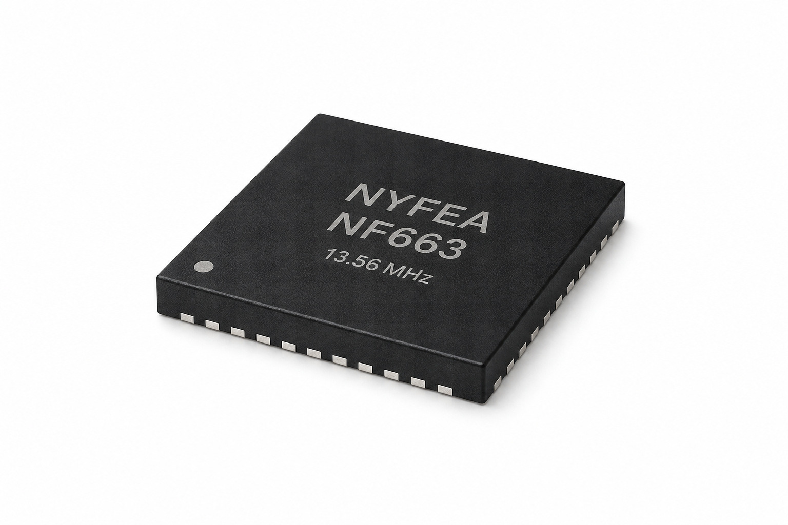
Why consider NF663 as a CLRC66303HNY alternative?
NF663 may reduce PCB rework because its published package and pin assignments align with the primary CLRC66303HNY signal map while retaining the core functions of a host-controlled 13.56 MHz reader.
- PCB starting point: the published HVQFN32 package and terminal assignments allow engineers to review an existing design without first remapping every signal.
- Reader resources: multi-protocol operation, SPI, I²C, UART, FIFO, EEPROM, power management and balanced RF interfaces remain available for engineering evaluation.
- Evaluation path: the NF663 specification, product information and sample process support a staged document review, prototype build and qualification program.
Commercial boundary: request current pricing, minimum order quantity, lead time and documentation availability.
Review the NYFEA NF663 technical information and request samples for a migration build.
What does NF663 provide beyond package and pin alignment?
NF663 integrates the control, timing, memory and low-power resources expected in a host-controlled NFC/HF RFID reader frontend. These resources support systematic firmware porting after basic host communication has been established.
These current values are typical IC-level figures, not guaranteed end-product limits. Measure the complete assembly with its MCU, regulator, antenna network and final LPCD duty cycle.
Firmware and prototype migration from CLRC66303HNY to NF663
Do not assume that CLRC66303HNY register-level firmware will run unchanged on NF663. Compare reset defaults and interface startup first, then review register semantics, EEPROM and FIFO organization, commands, IRQ and timer behavior, protocol configuration, error recovery, LPCD and security integration.
- Power and clock: verify every rail, reset state, interface strap and the 27.12 MHz clock.
- Host communication: read a register with a known reset value, then confirm one write-and-readback transaction.
- RF and protocol: confirm transmitter enable, field generation and one required card transaction before optimizing read range.
- Application behavior: test anticollision, authentication, data access, error recovery and every production credential type.
For fault isolation, capture the first transceive command, IRQ0 and IRQ1 status, FIFO length and returned bytes. A successful UID read confirms card discovery only; it does not verify protected-data access, longer responses or write transactions. See the NF663 reader board bring-up guide for the detailed diagnostic sequence.
How should CLRC66303HNY SPI firmware be ported to NF663?
Port the NF663 transport and reset layer before reusing higher-level CLRC66303HNY command flows. First verify a register read with a known reset value, a write-and-readback operation, FIFO access, bounded IRQ handling and error recovery. Then add protocol loading and target-card transactions.
NF663 places the seven-bit register address in SPI address-byte bits 7:1 and uses bit 0 as the read/write flag: 1 for read and 0 for write. Start with SPI mode 0, MSB first, and an SPI bit rate no higher than the specified 10 Mbit/s limit. The optional C99 example keeps GPIO, SPI and timing behind four hardware-abstraction callbacks for MCU portability.
Show the NF663 register map and portable C99 SPI example
| Item | Value | Purpose |
|---|---|---|
| Command / FIFOControl / FIFOLength / FIFOData | 0x00 / 0x02 / 0x04 / 0x05 | Command execution and FIFO access |
| IRQ0 / IRQ1 / Error | 0x06 / 0x07 / 0x0A | Completion, timer and error status |
| Version | 0x7F | Basic communication check |
| Idle / Transceive / LoadProtocol / SoftReset | 0x00 / 0x07 / 0x0D / 0x1F | Commands used during bring-up |
#include <stdbool.h>
#include <stddef.h>
#include <stdint.h>

typedef struct {
    bool (*spi_write)(const uint8_t *data, size_t length);
    bool (*spi_exchange)(const uint8_t *tx, uint8_t *rx, size_t length);
    void (*nss)(bool high);          /* false = select NF663 */
    uint32_t (*millis)(void);
} nf663_t;

enum {
    NF663_REG_COMMAND      = 0x00,
    NF663_REG_FIFO_CONTROL = 0x02,
    NF663_REG_FIFO_LENGTH  = 0x04,
    NF663_REG_FIFO_DATA    = 0x05,
    NF663_REG_IRQ0         = 0x06,
    NF663_REG_IRQ1         = 0x07,
    NF663_REG_ERROR        = 0x0A,
    NF663_REG_VERSION      = 0x7F
};

enum {
    NF663_CMD_IDLE          = 0x00,
    NF663_CMD_TRANSCEIVE    = 0x07,
    NF663_CMD_LOAD_PROTOCOL = 0x0D,
    NF663_CMD_SOFT_RESET    = 0x1F
};

enum {
    NF663_FIFO_FLUSH = 0x10,
    NF663_IRQ0_IDLE  = 0x10,
    NF663_IRQ0_RX    = 0x04,
    NF663_IRQ0_ERR   = 0x02
};

typedef enum {
    NF663_OK = 0,
    NF663_E_IO,
    NF663_E_TIMEOUT,
    NF663_E_CHIP,
    NF663_E_BUFFER
} nf663_status_t;

static uint8_t nf663_spi_address(uint8_t reg, bool read)
{
    return (uint8_t)((reg << 1) | (read ? 1u : 0u));
}

static bool nf663_write_reg(nf663_t *dev, uint8_t reg, uint8_t value)
{
    const uint8_t frame[2] = { nf663_spi_address(reg, false), value };
    dev->nss(false);
    const bool ok = dev->spi_write(frame, sizeof frame);
    dev->nss(true);
    return ok;
}

static bool nf663_read_reg(nf663_t *dev, uint8_t reg, uint8_t *value)
{
    const uint8_t address = nf663_spi_address(reg, true);
    const uint8_t dummy = 0x00;
    dev->nss(false);
    bool ok = dev->spi_write(&address, 1);
    if (ok) ok = dev->spi_exchange(&dummy, value, 1);
    dev->nss(true);
    return ok;
}

static bool nf663_fifo_write(nf663_t *dev,
                             const uint8_t *data, size_t length)
{
    const uint8_t address = nf663_spi_address(NF663_REG_FIFO_DATA, false);
    dev->nss(false);
    bool ok = dev->spi_write(&address, 1);
    if (ok && length != 0u) ok = dev->spi_write(data, length);
    dev->nss(true);
    return ok;
}

static bool nf663_fifo_read(nf663_t *dev, uint8_t *data, size_t length)
{
    const uint8_t address = nf663_spi_address(NF663_REG_FIFO_DATA, true);
    const uint8_t dummy = 0x00;
    dev->nss(false);
    bool ok = dev->spi_write(&address, 1);
    for (size_t i = 0; ok && i < length; ++i)
        ok = dev->spi_exchange(&dummy, &data[i], 1);
    dev->nss(true);
    return ok;
}

static bool nf663_flush_fifo(nf663_t *dev)
{
    uint8_t control;
    return nf663_read_reg(dev, NF663_REG_FIFO_CONTROL, &control) &&
           nf663_write_reg(dev, NF663_REG_FIFO_CONTROL,
                           (uint8_t)(control | NF663_FIFO_FLUSH));
}

bool nf663_read_version(nf663_t *dev, uint8_t *version)
{
    return nf663_read_reg(dev, NF663_REG_VERSION, version);
}

bool nf663_soft_reset(nf663_t *dev)
{
    return nf663_write_reg(dev, NF663_REG_COMMAND,
                           NF663_CMD_SOFT_RESET);
}

bool nf663_load_protocol(nf663_t *dev,
                         uint8_t rx_protocol, uint8_t tx_protocol)
{
    const uint8_t parameters[2] = { rx_protocol, tx_protocol };
    return nf663_write_reg(dev, NF663_REG_COMMAND, NF663_CMD_IDLE) &&
           nf663_flush_fifo(dev) &&
           nf663_fifo_write(dev, parameters, sizeof parameters) &&
           nf663_write_reg(dev, NF663_REG_COMMAND,
                           NF663_CMD_LOAD_PROTOCOL);
}

nf663_status_t nf663_transceive(nf663_t *dev,
                                const uint8_t *tx, size_t tx_length,
                                uint8_t *rx, size_t *rx_length,
                                uint32_t timeout_ms,
                                uint8_t *chip_error)
{
    uint8_t irq0, error, fifo_control, fifo_length;

    if (!tx || !rx || !rx_length || tx_length > 512u)
        return NF663_E_BUFFER;

    if (!nf663_write_reg(dev, NF663_REG_COMMAND, NF663_CMD_IDLE) ||
        !nf663_flush_fifo(dev) ||
        !nf663_write_reg(dev, NF663_REG_IRQ0, 0x7F) ||
        !nf663_write_reg(dev, NF663_REG_IRQ1, 0x7F) ||
        !nf663_fifo_write(dev, tx, tx_length) ||
        !nf663_write_reg(dev, NF663_REG_COMMAND, NF663_CMD_TRANSCEIVE))
        return NF663_E_IO;

    const uint32_t start = dev->millis();
    for (;;) {
        if (!nf663_read_reg(dev, NF663_REG_IRQ0, &irq0))
            return NF663_E_IO;
        if ((irq0 & NF663_IRQ0_ERR) != 0u) break;
        if ((irq0 & (NF663_IRQ0_RX | NF663_IRQ0_IDLE)) != 0u) break;
        if ((uint32_t)(dev->millis() - start) >= timeout_ms) {
            (void)nf663_write_reg(dev, NF663_REG_COMMAND, NF663_CMD_IDLE);
            return NF663_E_TIMEOUT;
        }
    }

    if (!nf663_read_reg(dev, NF663_REG_ERROR, &error))
        return NF663_E_IO;
    if (chip_error) *chip_error = error;
    if (error != 0u) return NF663_E_CHIP;

    if (!nf663_read_reg(dev, NF663_REG_FIFO_CONTROL, &fifo_control) ||
        !nf663_read_reg(dev, NF663_REG_FIFO_LENGTH, &fifo_length))
        return NF663_E_IO;

    const size_t available =
        ((size_t)(fifo_control & 0x03u) << 8) | fifo_length;
    if (available > *rx_length) {
        *rx_length = available;
        return NF663_E_BUFFER;
    }

    *rx_length = available;
    if (available != 0u && !nf663_fifo_read(dev, rx, available))
        return NF663_E_IO;

    return NF663_OK;
}
Scope boundary: this example covers transport and command sequencing only; it is neither a complete ISO/IEC 14443 stack nor production-qualified firmware. Before calling nf663_transceive(), the application must load the required protocol and configure framing, CRC, bit handling, timeouts and RF settings. The cited NF663 specification assigns RX protocol 0 and TX protocol 0 to ISO/IEC 14443 Type A at 106 kbit/s when using LoadProtocol. Confirm these values against the revision-controlled specification for the project.
NF663 PCB reference design: what it can and cannot establish
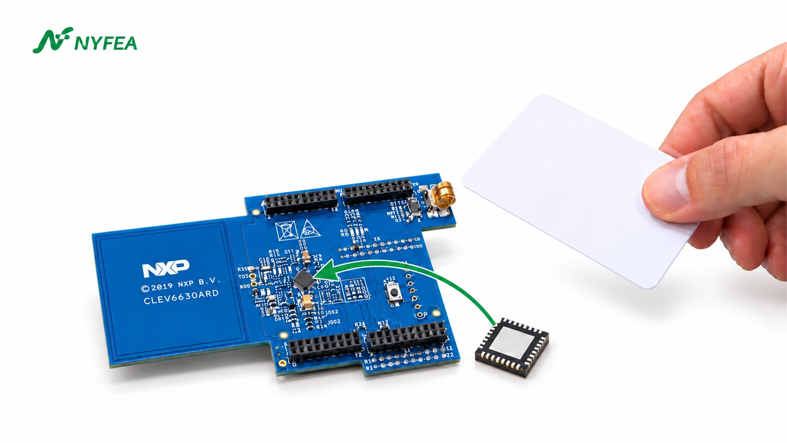
Treat the assembled-board and zoning images below as layout and bring-up references. They show how to separate the host interface, reader IC, clock, power, balanced transmitter network and antenna for measurement; they do not establish a production-qualified implementation.
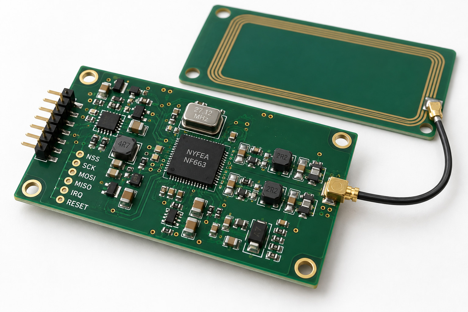
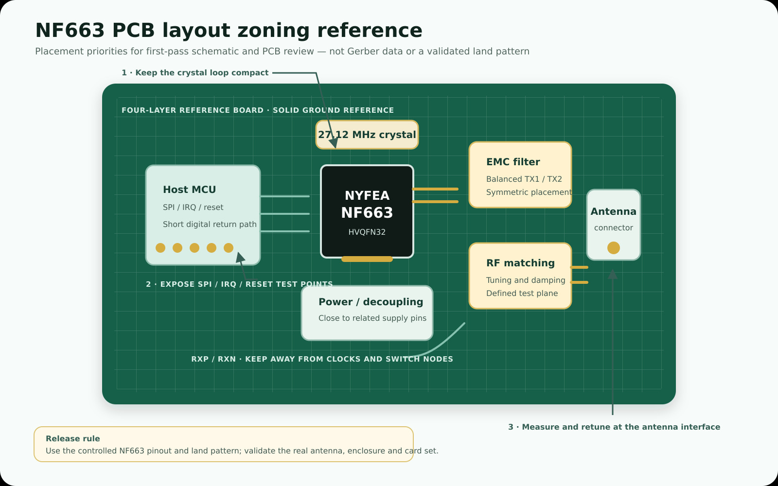
 Power domainsKeep VDD, PVDD and TVDD within the specified 3.0 V to 5.5 V range. Place local decoupling at the relevant pins, then measure startup behavior, ripple and transmitter-current headroom on the assembled board.
 ClockPlace the 27.12 MHz crystal and its load network close to XTAL1 and XTAL2. The published reference specifies 10 pF load capacitance, ±250 ppm frequency tolerance and ESR up to 100 Ω; verify the selected crystal and PCB parasitics.
 Host interfaceRoute SPI over a continuous return path and provide accessible test points for NSS, SCK, MOSI, MISO, IRQ and reset. Begin with SPI mode 0, MSB first, and remain within the 10 Mbit/s limit.
 RF pathRoute TX1 and TX2 symmetrically through the EMC filter and matching network. Treat RXP, RXN and VMID as sensitive analog nodes, separated from clocks, switching-regulator nodes and fast digital edges.
 Antenna interfaceDefine the impedance-measurement plane at the antenna connector or matching network. Do not copy CLRC66303HNY component values without measuring the antenna and retuning the complete RF path.
 Release evidenceArchive the board revision, stack-up, schematic, matching-network BOM, antenna impedance, current waveforms, card matrix, firmware commit, temperature and enclosure state.
Bring-up should progress from rail and clock verification to register access, IRQ and FIFO behavior, RF field generation, and the complete required-card matrix.
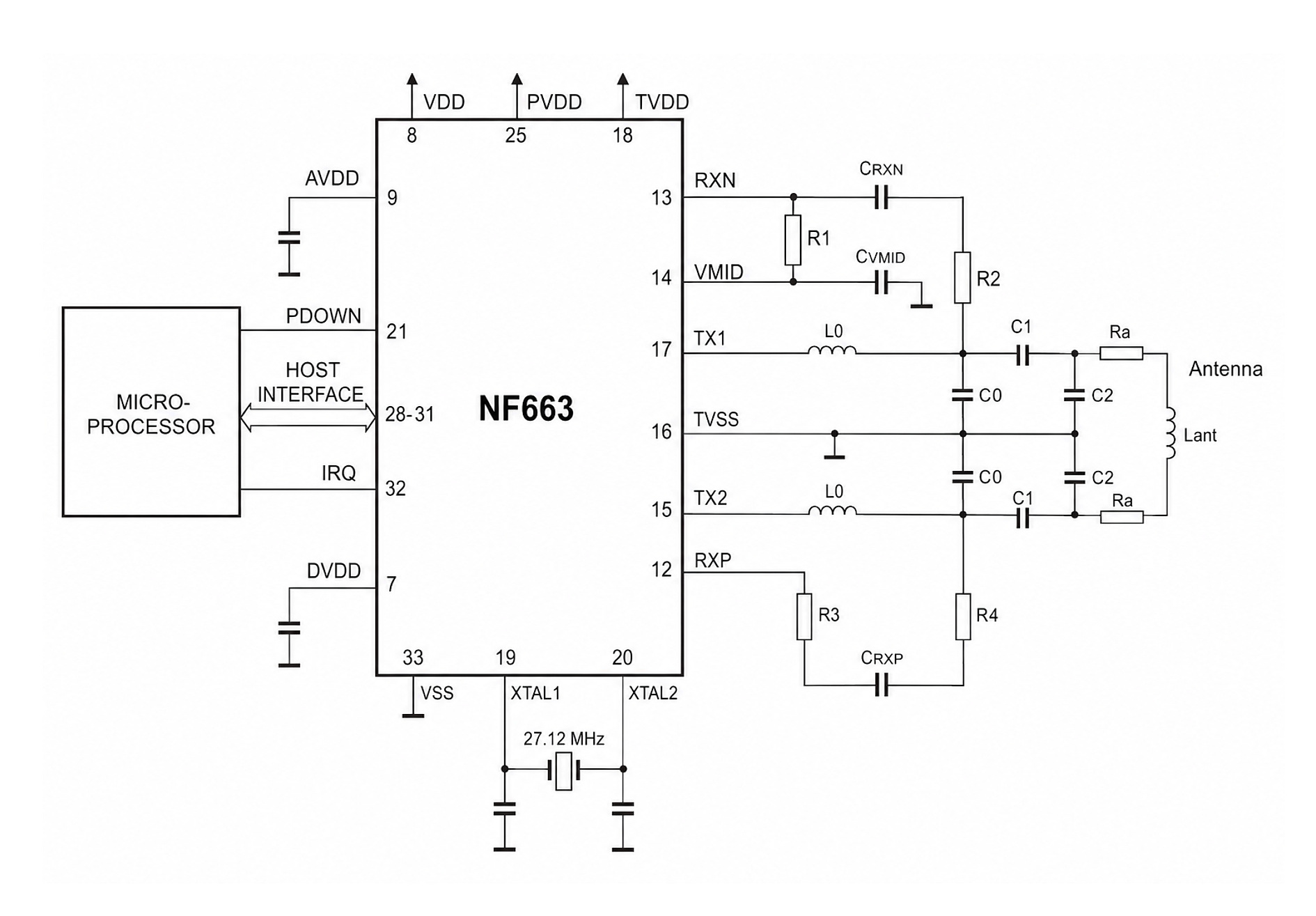
Can the CLRC66303HNY antenna and LPCD settings be reused with NF663?
Do not release an NF663 design using unverified CLRC66303HNY RF component values or LPCD thresholds. The antenna geometry may be retained as a controlled starting point, but the filter, matching network, receiver path and low-power detection behavior must be characterized again.
Normal communication range and LPCD wake range require separate acceptance criteria. Measure antenna impedance at a documented calibration plane, transmitter current and waveform, receiver margin, card-transaction success, LPCD I/Q baseline, false-wake rate, missed-card rate and wake-to-transaction time. Repeat the tests with the final enclosure, battery, display, cables, ferrite, nearby metal and required cards.
For the detailed method, use the CLRC663 antenna and read-range guide and the CLRC663 LPCD I/Q register debugging guide.
How should an NF663 migration be qualified for release?
The release workflow should convert every compatibility claim into a requirement, test method, result and responsible owner. A feature comparison can screen a candidate; design approval requires documented qualification.
| Gate | Evidence to collect | Minimum exit condition |
|---|---|---|
| 1. Baseline | CLRC66303HNY order code, schematic, BOM, PCB, firmware, cards, antenna, operating limits and known failure modes | One revision-controlled baseline for the exact CLRC66303HNY configuration |
| 2. Gap review | Pin-by-pin, rail-by-rail, command, register, timing, RF and qualification matrix | Every item classified as aligned, different or requiring a test, with a cited source |
| 3. Prototype | NF663 schematic, PCB, RF network, firmware port and bring-up log | Stable register access, controlled RF operation and repeatable fault recovery |
| 4. Interoperability | Card/tag matrix, orientation grid, distance distribution, protocol transactions, collision and security cases | All required credentials meet the written acceptance limits |
| 5. Power and LPCD | Current by state, duty cycle, false wakes, missed cards, latency, temperature and nearby-object effects | Product-level energy and detection criteria pass under the specified conditions |
| 6. Production | Corner samples, RF tolerance, EMC/ESD results, programming, traceability, yield and end-of-line test | Approved release package with component, firmware and manufacturing revision control |
Make each test reproducible: record the board serial number and revision, firmware commit, antenna and matching-network BOM, card model, supply voltage, temperature, orientation, distance, trial count, failures and recovery behavior. Define pass criteria before testing. For LPCD, report false wakes per observation period and missed detections per presentation count together with current consumption and wake latency.
Preserve raw logs and failed cases. A documented failure is more useful than an isolated “works” result because it defines a repeatable boundary condition and a measurable target for the next revision.

CLRC66303HNY replacement FAQ
What is a replacement for CLRC66303HNY?
NF663 is an evaluation candidate because the published package and pin assignments align closely. It is not a production-approved drop-in replacement; apply the selection gates before building a prototype.
Is NF663 pin-compatible with CLRC66303HNY?
The published pin numbers and primary signal names align. Confirm electrical behavior, land pattern, solder-paste design and assembly requirements during the pin review.
Can NF663 use the existing CLRC66303HNY PCB?
The existing PCB may be used as a prototype starting point after every net, supply rail, strap and external component has been reviewed. Follow the PCB evaluation guidance.
Is CLRC66303HNY active or obsolete?
NXP listed CLRC66303HN as Active when this article was updated. Verify the exact orderable status and authorized-channel availability when purchasing.
What does the HNY suffix mean?
HNY identifies the wettable-flank HVQFN32 reel option. See the ordering summary for package and delivery details.
Can existing CLRC66303HNY firmware be reused with NF663?
Direct reuse should not be assumed. Port and verify interface startup, register access, commands, FIFO, IRQ, timers, protocol loading and error recovery using the firmware migration steps.
What read range should be expected from NF663?
The specification gives a typical reference of up to 12 cm under its stated conditions. Measure the finished product with the final antenna, enclosure and required cards as described in the RF validation section.
Primary technical sources
- NXP CLRC663 data sheet, Rev. 5.4 — specifications, limits, package and ordering.
- NXP CLRC663 plus product page — lifecycle and development resources.
- NXP AN12657 — host-interface commands and protocol examples.
- NXP AN11019 — antenna matching and measurement.
- NXP AN11145 — LPCD design and tuning.
- NYFEA NF663 product page and product specification — NF663 specifications, pins, registers and RF guidance.
Engineering basis: Use revision-controlled manufacturer specifications for design decisions and qualify NF663 on the target hardware before release.
Disclosure: NYFEA supplies NF663.
Evaluate NF663 against your CLRC66303HNY design requirements
For a project-specific migration review, provide the required quantity, supply voltage, temperature range, MCU, host interface, target cards, antenna and read-zone requirements, and identify whether the PCB or firmware may change.
CLRC66303HNY, CLRC663, NXP, MIFARE, FeliCa, ICODE and related names or marks belong to their respective owners. NF663 is a NYFEA product. NYFEA and NF663 are not affiliated with, endorsed by or sponsored by NXP. Third-party names identify engineering context only.