MFRC52202HN1 End of Life: Datasheet Facts, Replacement Risks and an NF522 Migration Guide
Identify the exact MFRC52202HN1 Version 2.0 device, understand its lifecycle status and choose a defensible redesign route before qualifying an NF522-based 13.56 MHz reader.
DIRECT ANSWER
MFRC52202HN1 is the Version 2.0 device in the MFRC522 family. It operates at 13.56 MHz, supports ISO/IEC 14443 Type A, MIFARE and NTAG, and uses a 5 × 5 × 0.85 mm HVQFN32 package. NXP currently marks MFRC52202HN1 End of Life and not recommended for new designs, with CLRC663 plus named as the recommended NXP new-design product.
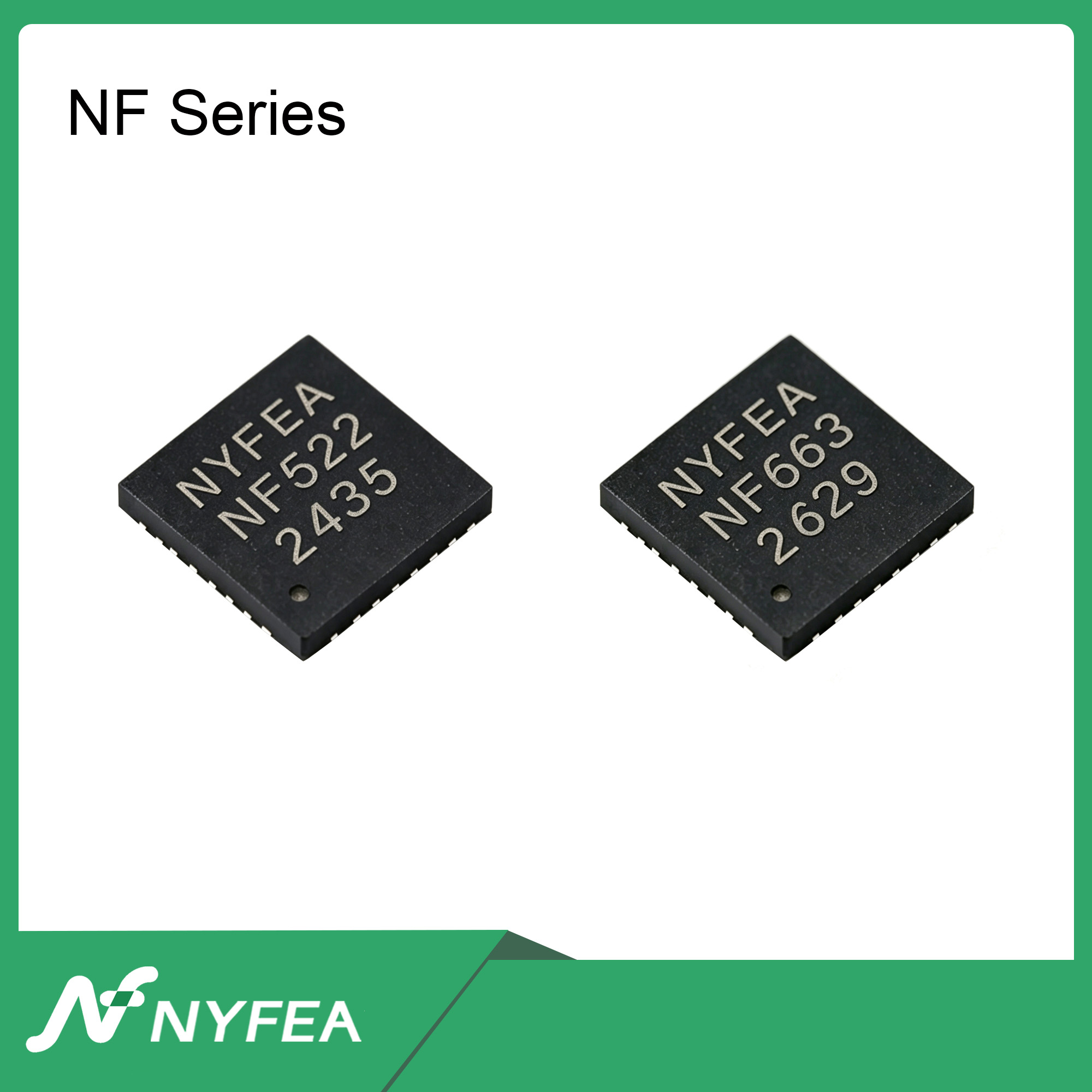
NF522 is a separate NYFEA reader IC that may be evaluated for a redesigned product, particularly where Type B, ISO/IEC 15693 or low-power card detection is required. It must not be described as pin-to-pin, register-level or firmware-compatible with MFRC52202HN1 unless that result has been established for the specific design.
Engineers searching for “MFRC52202HN1 datasheet,” “MFRC52202HN1 EOL,” “MFRC52202HN1 replacement” or “MFRC52202HN1 alternative” are usually maintaining an existing BOM, checking a device revision or planning a redesign. This guide first establishes the verified MFRC52202HN1 baseline, then compares three lifecycle routes and defines the hardware, firmware and RF evidence required before NF522 can be approved.
| Question | Engineering answer |
|---|---|
| What is MFRC52202HN1? | The Version 2.0 device in the MFRC522 reader-IC family. |
| Is it End of Life? | Yes. NXP currently marks the ordering code End of Life. |
| What does NXP recommend? | CLRC663 plus for new designs. |
| Where does NF522 fit? | As an independent candidate for a new or redesigned reader, subject to complete qualification. |
| What must be revalidated? | Package and pins, power, host transactions, registers, firmware, RF matching, cards, EMC and production performance. |
1. What exactly is MFRC52202HN1?
MFRC52202HN1 is not the name of a common blue “RC522 module.” It is a specific reader IC: Version 2.0 of the MFRC522 family. The IC operates at 13.56 MHz and integrates RF transmission, receive demodulation, ISO/IEC 14443 Type A framing, parity and CRC processing, a 64-byte FIFO, programmable timing, interrupts and host-interface control.
The device supports SPI, I²C and serial UART host interfaces. It uses the HVQFN32 SOT617-1 package, with a 5 × 5 × 0.85 mm body. A complete reader still requires a host MCU, clock source, power and decoupling, reset and interrupt circuitry, an antenna and matching network, firmware, security logic and final-system qualification.
Do not confuse three different identifiers
- MFRC522: the reader-IC family.
- MFRC52202HN1: the Version 2.0 device type.
- RC522 module: a board-level product that may add an antenna, matching parts, crystal, connector and power components.
BOM control, lifecycle review and PCB migration must use the exact IC ordering information and controlled documentation—not a module nickname or search-market description.
2. MFRC52202HN1 vs MFRC52201HN1
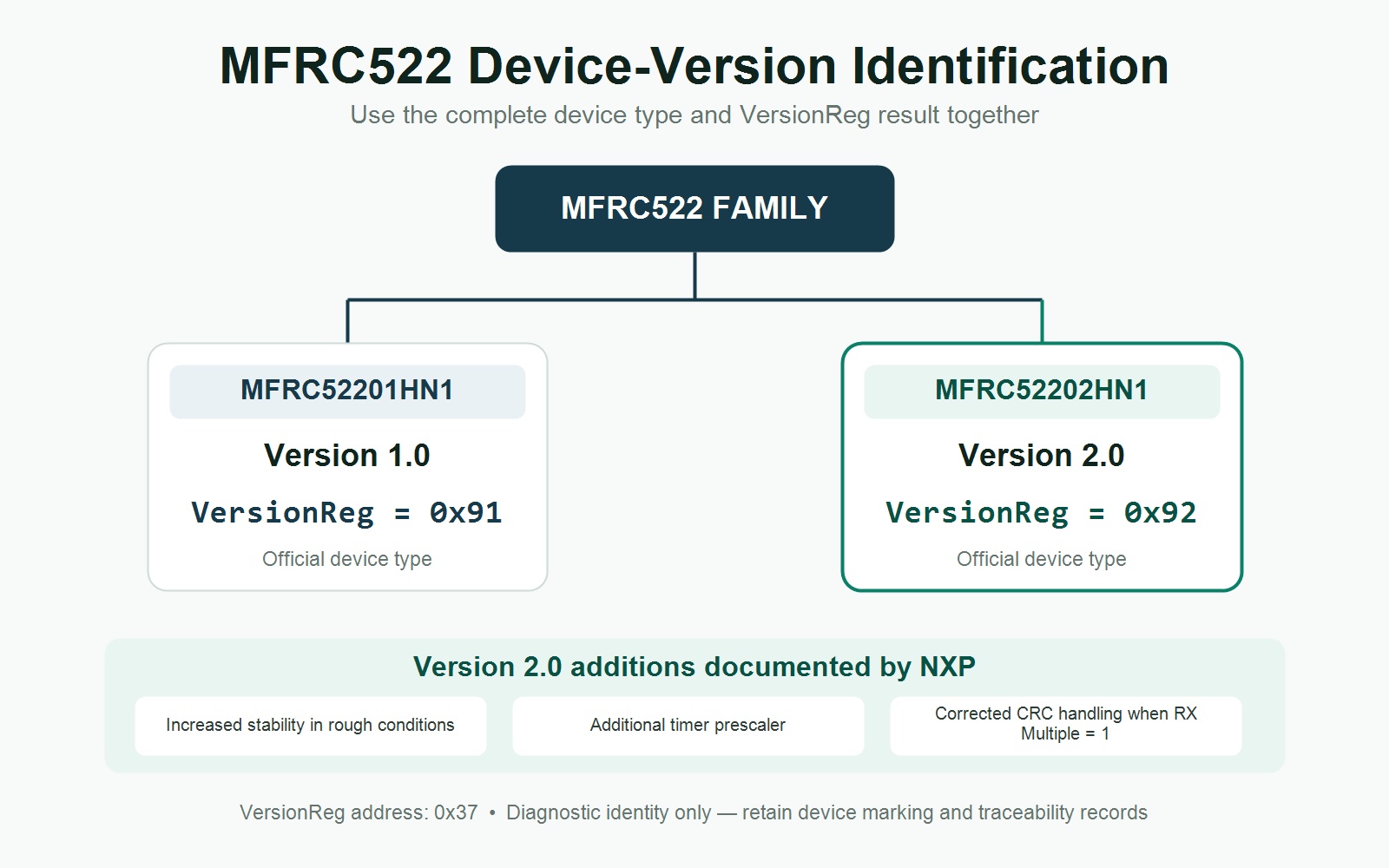
NXP identifies MFRC52201HN1 as Version 1.0 and MFRC52202HN1 as Version 2.0. Within the official MFRC522 family, NXP documents Version 2.0 as fully compatible with Version 1.0 and lists three additions or improvements:
- increased reader-IC stability under rough operating conditions;
- an additional timer prescaler; and
- corrected CRC handling when
RX Multipleis set to 1.
Firmware can read VersionReg at address 0x37: the documented value is 0x91 for Version 1.0 and 0x92 for Version 2.0. This is useful for startup diagnostics and production tests, but it does not replace device marking, purchase traceability or supplier quality controls.
uint8_t version = read_register(0x37);

if (version == 0x92) {
    /* MFRC522 Version 2.0: MFRC52202HN1 */
} else if (version == 0x91) {
    /* MFRC522 Version 1.0: MFRC52201HN1 */
}
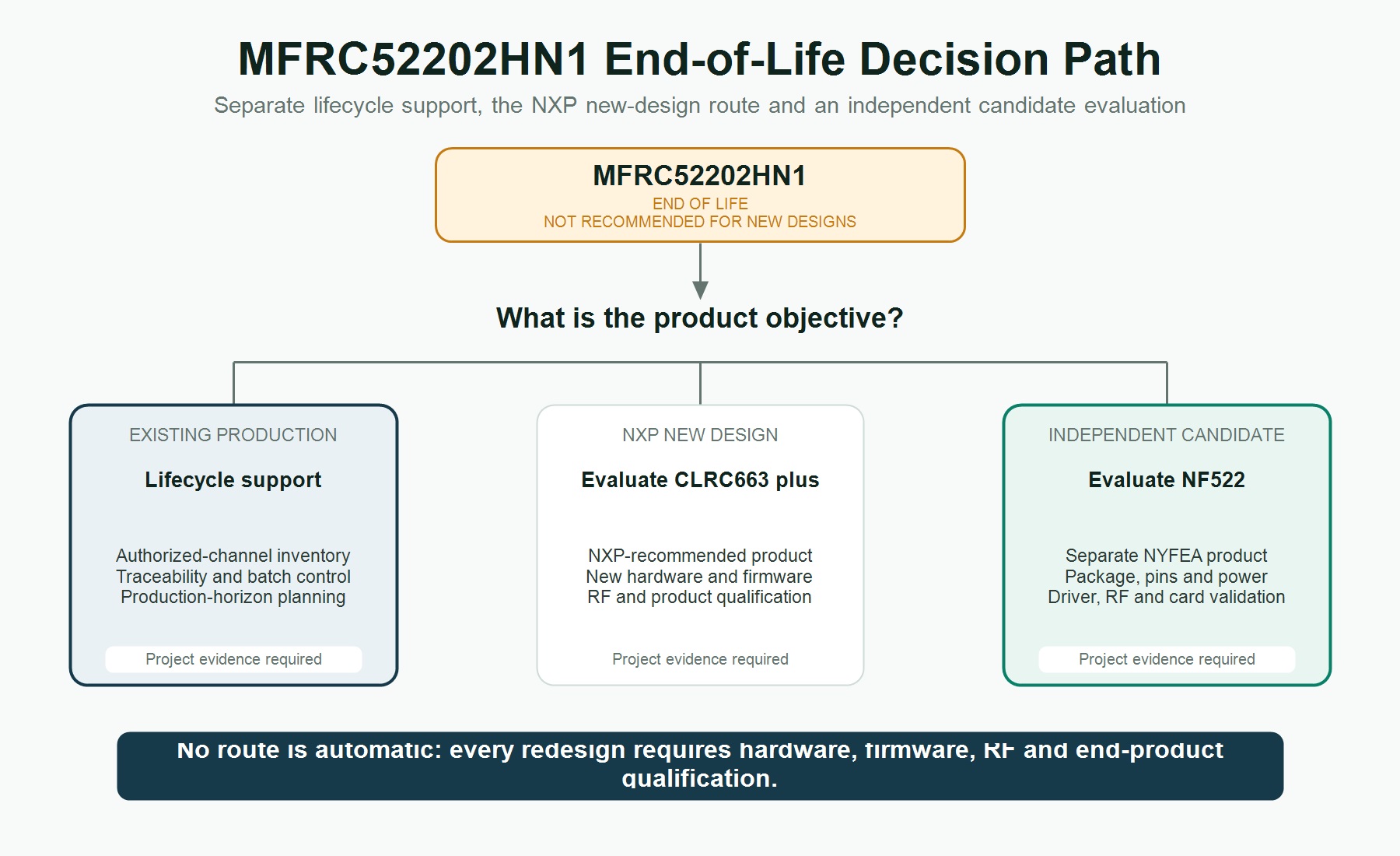
3. Three routes after MFRC52202HN1 End of Life
NXP currently marks MFRC52202HN1 End of Life and not recommended for new designs. The same product page names CLRC663 plus as the recommended NXP new-design product. An engineering team should separate three distinct routes rather than treating every lifecycle problem as a search for a “drop-in replacement.”
| Project condition | Route to evaluate | Primary work |
|---|---|---|
| Existing product cannot yet change | Authorized-channel inventory and lifecycle plan | Traceability, inventory risk, production horizon and revision control. |
| New design remains in the NXP ecosystem | Evaluate NXP-recommended CLRC663 plus | New hardware, firmware, RF and end-product qualification. |
| Project needs an independent candidate | Evaluate NF522 as a separate reader IC | Package, pins, power, software, RF and card-set validation. |
| Project needs Type B, ISO/IEC 15693 or LPCD | Review the corresponding NF522 capabilities | Add protocol, card, power-mode and wake-up tests. |
| PCB and firmware must remain unchanged | Do not promise a direct replacement without evidence | First establish compatibility or redesign constraints. |
4. Representative migration scenario: an access-control reader redesign
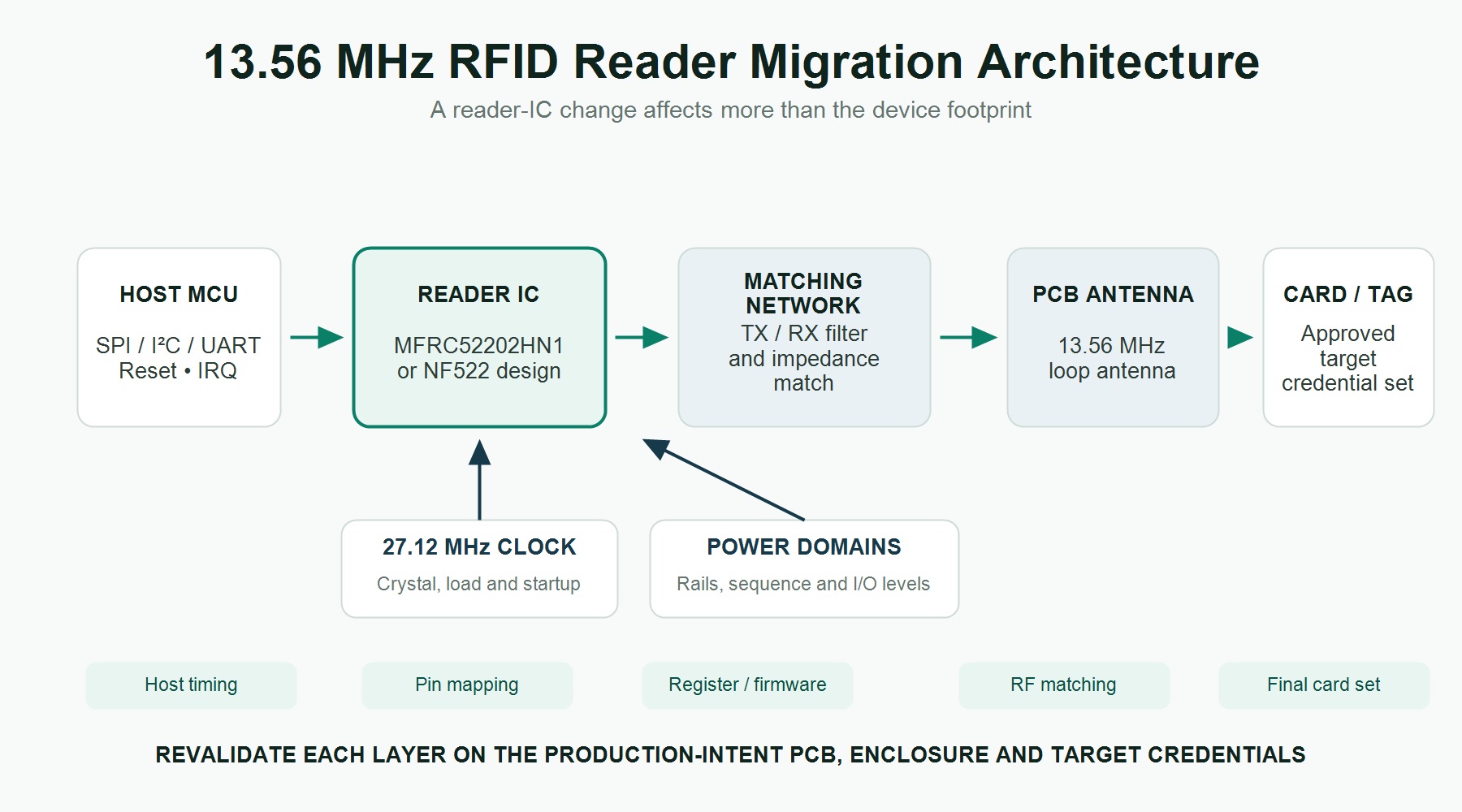
The following is a representative engineering scenario, not a claimed customer test result. An installed access-control terminal uses an MCU, SPI, reset and IRQ to control MFRC52202HN1. A 27.12 MHz clock, external matching network and PCB loop antenna complete the 13.56 MHz reader. Firmware performs polling, anti-collision, card selection, authentication and data access for approved ISO/IEC 14443 Type A credentials.
Host MCU
   ├── SPI / Reset / IRQ
   │
MFRC52202HN1
   ├── 27.12 MHz clock
   └── TX / RX network
            │
       Matching network
            │
        PCB antenna
            │
  ISO/IEC 14443 Type A card
The redesign objectives are to retain the approved Type A card set, keep the host platform where practical, reduce lifecycle exposure and leave room for Type B, ISO/IEC 15693 or low-power card detection in future variants. This is not a one-line BOM substitution. It is a controlled system migration spanning hardware, firmware, RF and production evidence.
5. Freeze the existing MFRC52202HN1 design baseline
Without a measured baseline, the team cannot tell whether a difference comes from the IC, driver, PCB, antenna or enclosure. Record the production-intent design before selecting any candidate.
| Item | Evidence to record |
|---|---|
| Exact device and revision | Full MFRC52202HN1 ordering information, marking, schematic and PCB revision. |
| Device identity | VersionReg result and production traceability records. |
| Target credentials | Card or tag type, protocol, UID format, security method and application data. |
| Host interface | SPI, I²C or UART selection, actual data rate, timing and logic levels. |
| Power architecture | Every rail, voltage, ripple, sequence, field-on current and sleep condition. |
| Clock | Crystal or clock-source part, load components, startup and routing. |
| Reset and interrupt | Polarity, timing, pull resistors, MCU connections and recovery sequence. |
| Firmware | Initialization, polling, anti-collision, authentication, timeout and fault recovery. |
| Antenna system | Geometry, turns, inductance, Q, matching BOM and final enclosure stack. |
| RF performance | Read-zone map, orientation, card set, supply condition and failure rate. |
| Compliance and production | EMC, temperature, reliability and manufacturing-test requirements. |
6. What NF522 adds to a redesigned reader
NF522 is a NYFEA 13.56 MHz multi-protocol RFID reader IC. The current technical page lists the following capabilities:
- ISO/IEC 14443 Type A reader mode;
- ISO/IEC 14443 Type B reader mode;
- ISO/IEC 15693 reader mode;
- SPI, I²C and UART host interfaces;
- a 64-byte transmit/receive FIFO;
- CRC16 generation and checking;
- a programmable timer and configurable interrupt;
- Hard Power-Down and Soft Power-Down;
- low-power card detection (LPCD);
- an oscillator circuit for an external 27.12 MHz crystal; and
- a QFN32 package.
These capabilities make NF522 relevant to a new or redesigned reader that needs broader protocol coverage or a defined low-power detection path. They do not establish an MFRC52202HN1-compatible footprint, pinout, register map, driver or antenna network.
7. Compare documented capability separately from migration compatibility
A useful comparison distinguishes three result types:
- Documented common capability: for example, both devices operate at 13.56 MHz and offer SPI, I²C and UART host options.
- Documented feature extension: NF522 additionally lists Type B, ISO/IEC 15693 and LPCD.
- Design-specific compatibility: package pads, pin assignments, power sequencing, transactions, registers, firmware and RF performance must be proved on the target design.
Read-range caution: maximum distance statements from different data sheets are not directly comparable unless antenna, matching, supply, card, enclosure and test method are held constant. This guide intentionally uses a controlled A/B measurement plan rather than ranking headline range figures.
8. MFRC52202HN1 and NF522 engineering comparison
The table below compares documented device-level facts. It is not a declaration of equivalence. Each common headline feature must be followed by a design-specific compatibility check.
Documented capabilities and migration meaning
| Design question | MFRC522 documented baseline | NF522 documented baseline | Migration meaning |
|---|---|---|---|
| Carrier frequency | 13.56 MHz | 13.56 MHz | The same frequency does not establish antenna, pin or firmware compatibility. |
| Reader protocols | ISO/IEC 14443 Type A, MIFARE and NTAG | ISO/IEC 14443 Type A, Type B and ISO/IEC 15693 reader modes; the data sheet also lists an M1 mode | NF522 can be evaluated where broader protocol coverage is required; validate card technology, licensing, security and software flow. |
| Type A data rates | 106, 212, 424 and 848 kBd | 106, 212, 424 and 848 kbit/s | Matching headline rates do not prove matching register configuration or timing behavior. |
| Host interfaces | SPI, I²C and serial UART | SPI, I²C and UART | Validate transaction framing, modes, address selection, timing, reset and I/O levels. |
| Maximum documented SPI rate | 10 Mbit/s | 12 Mbit/s | Choose a rate proven on the target MCU, routing and firmware; maximum figures are not a migration setting. |
| FIFO | 64-byte shared transmit/receive FIFO | 64-byte transmit/receive FIFO | Revalidate FIFO commands, status, errors and interrupt handling. |
| Reference clock | 27.12 MHz crystal connection | External 27.12 MHz crystal | Recheck oscillator network, startup and layout against the selected device data sheet. |
| Package description | HVQFN32, 5 × 5 mm | QFN32 | A similar pin count is not proof of the same footprint, exposed pad or pin assignment. |
| Operating temperature | −25°C to +85°C ambient | −25°C to +85°C ambient | System qualification is still required across the final power and RF conditions. |
Comparison boundary: values above come from the controlled MFRC522 and NF522 technical documents available during this review. Confirm the latest ordering code, document revision and application requirements before design approval. Read-distance numbers are intentionally excluded because they are not comparable without the same antenna, card, enclosure and test method.
9. A controlled MFRC52202HN1-to-NF522 migration sequence
NF522 may be evaluated for a new or redesigned 13.56 MHz reader, especially when Type B or ISO/IEC 15693 reader modes are required in addition to Type A. The current NF522 technical information does not state MFRC52202HN1 pin-to-pin, footprint, register-map, firmware or antenna-network compatibility. A defensible project decision therefore requires the following sequence:
- Freeze the MFRC522 baseline: save the schematic, PCB, antenna dimensions, BOM, firmware revision, card set and measured read-zone results.
- Compare the package and every pin: include exposed pad, power and ground pins, TX/RX, clock, reset, IRQ and interface-selection pins.
- Compare all power domains: check operating ranges, sequencing, I/O thresholds, decoupling and field-on current—not only the label “3.3 V.”
- Audit host transactions: verify SPI framing and mode, I²C address and timing or UART startup behavior with a logic analyzer.
- Port by function, not by assumption: implement an NF522 low-level driver behind a common reader API; validate reset values, commands, FIFO, timer, CRC, interrupts and error handling against NF522 documentation.
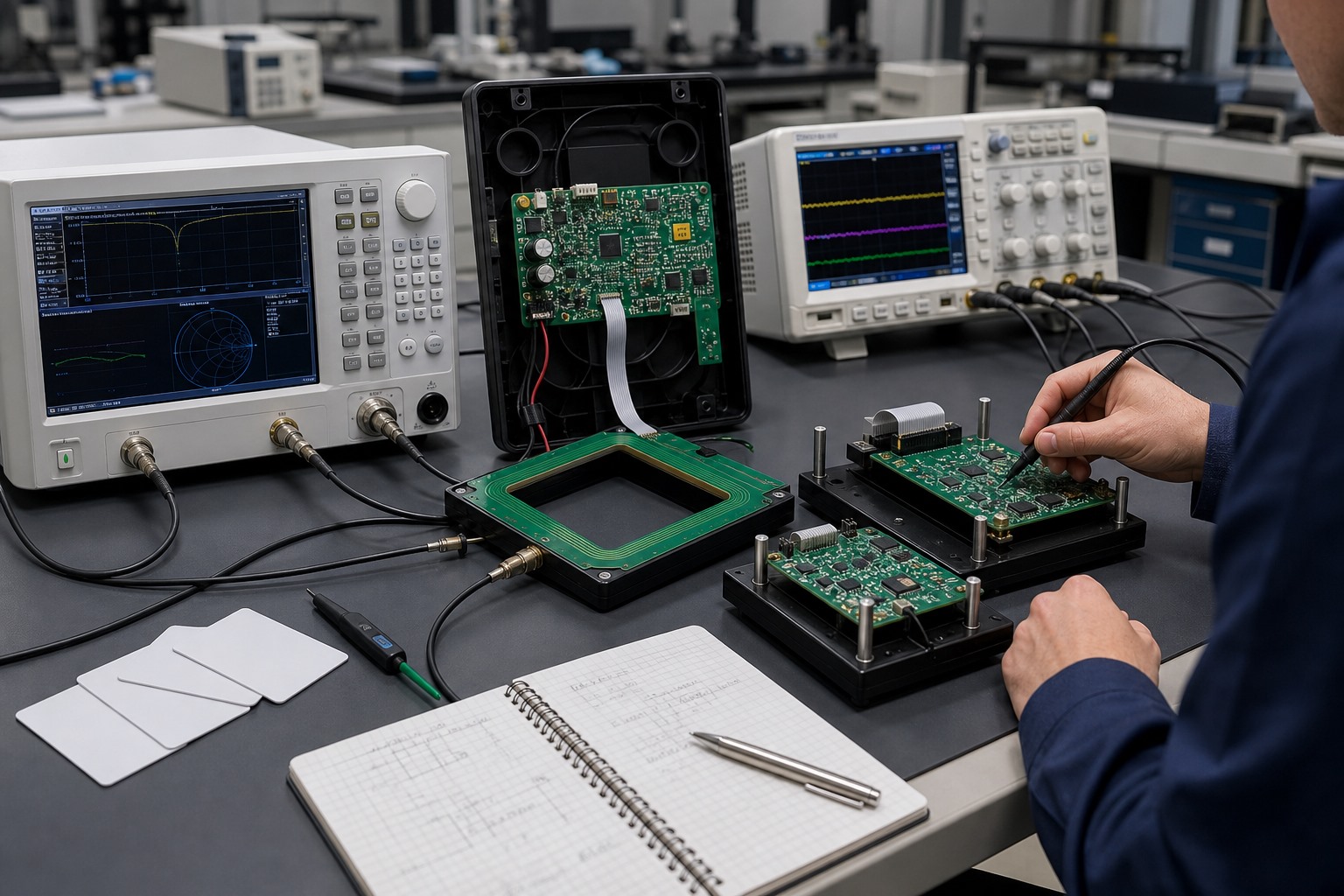
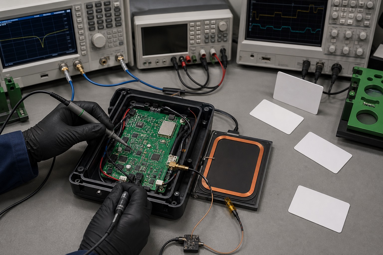
- Retune the RF system: keep the old antenna geometry only as a starting point; measure the matching network on the NF522 PCB in the final enclosure.
- Run an A/B qualification: compare cold start, sleep and wake, card detection, read zone, noise immunity, temperature and recovery using the same production-intent test plan.
Recommended firmware structure
Application
    │
Common RFID Reader API
    │
    ├── MFRC522 Driver
    └── NF522 Driver
A common application API preserves business states and error policy while keeping register-level behavior device-specific. It also supports controlled A/B testing and clearer hardware-revision management.
10. What can be reused, and what must be revalidated?
| Potentially reusable engineering asset | Mandatory revalidation |
|---|---|
| Product requirements and supported-card list | NF522 protocol configuration and end-to-end card transactions |
| Position/orientation read-zone test fixture | Pass limits using the NF522 board and final enclosure |
| Antenna outline as an initial geometry | EMC filter, matching values, impedance, field strength and receive margin |
| Host-side application states and error policy | Driver, register accesses, commands, IRQ, timer, CRC and FIFO behavior |
| Manufacturing traceability and test concept | NF522-specific test points, diagnostics, limits and golden-board references |
11. Production-oriented acceptance and evidence
- Cold-start and reset recovery are repeatable
- Register identification and bus transactions are stable
- Required Type A, Type B and/or ISO/IEC 15693 cards pass
- Timeout, card removal and error recovery do not require a power cycle
- Read-zone coverage meets the product requirement in the enclosure
- Display, converter, cable and radio noise are active during RF tests
- Low-power entry, wake source and wake latency are measured at system level
- Production component tolerances and antenna variation are represented
- Temperature and supply corners use documented pass criteria
- Firmware and hardware revisions are traceable in every result
Do not approve an MFRC52202HN1-to-NF522 migration because one card produces one UID on an open bench. Approve it when the NF522 design passes the same controlled product requirements with documented margin.
Migration validation record
| Test | MFRC52202HN1 baseline | NF522 prototype | Acceptance criterion |
|---|---|---|---|
| Cold-start success rate | Measure | Measure | Meets the product requirement. |
| Warm-reset success rate | Measure | Measure | Meets the product requirement. |
| Reference-card read distance | Measure | Measure | Compared under the same fixture and conditions. |
| Position and orientation coverage | Map | Map | Passes the defined read zone. |
| Repeated-card event handling | Record | Record | Matches the application state machine. |
| Multi-card anti-collision | Record | Record | Required behavior is repeatable. |
| CRC and timeout recovery | Record | Record | Automatic recovery without a power cycle. |
| Brownout recovery | Record | Record | Returns to a defined reader state. |
| Low- and high-temperature operation | Measure | Measure | Meets end-product limits. |
| Complete-system standby current | Measure | Measure | Meets the system power budget. |
| EMC result | Record | Record | Meets the target standard. |
Engineering FAQs
Is MFRC52202HN1 End of Life?
Yes. NXP currently marks MFRC52202HN1 End of Life and not recommended for new designs.
Which device does NXP recommend for a new design?
The current NXP product page recommends CLRC663 plus. This is the NXP new-design route, but project-specific hardware, firmware, RF and end-product qualification are still required.
What is the difference between MFRC52202HN1 and MFRC52201HN1?
MFRC52201HN1 is Version 1.0 and MFRC52202HN1 is Version 2.0. NXP documents Version 2.0 as compatible with Version 1.0 within the official MFRC522 family and adds stability, timer-prescaler and specific CRC-handling improvements.
What package does MFRC52202HN1 use?
MFRC52202HN1 uses an HVQFN32 SOT617-1 package with a 5 × 5 × 0.85 mm body. Use the current controlled package drawing for PCB design.
How can firmware identify MFRC522 Version 2.0?
Read VersionReg at address 0x37. NXP documents 0x91 for MFRC522 Version 1.0 and 0x92 for Version 2.0.
Which protocols does MFRC52202HN1 support?
MFRC52202HN1 supports 13.56 MHz ISO/IEC 14443 Type A, MIFARE and NTAG communication. End-product card support also depends on the credential, security architecture, firmware and qualification requirements.
Can NF522 directly replace MFRC52202HN1?
Do not assume a direct replacement. Verify package and pin mapping, power rails, host transactions, registers, firmware, RF matching, EMC and target-card performance for the specific design.
Can an existing MFRC522 driver be reused for NF522?
Reuse should not be assumed before the command and register architectures are compared. A separate NF522 low-level driver behind a common reader API is the safer migration structure.
What additional reader modes does NF522 provide?
The current NF522 technical page lists ISO/IEC 14443 Type A, Type B and ISO/IEC 15693 reader modes, together with low-power card detection. All functions require target-card, firmware, RF and product-level validation.
Review the controlled NF522 technical data
Use the current NF522 document for pin functions, electrical conditions, protocols, commands, register behavior and package information. This migration guide does not replace either manufacturer’s controlled technical documentation.
Download NF522 Technical Datasheet (PDF)
Planning an MFRC52202HN1 lifecycle redesign?
Share the approved card protocols, host interface, supply plan, antenna dimensions, enclosure stack and measured MFRC52202HN1 baseline with NYFEA. The productive first question is not “Is it drop-in?” but “Which requirements and interfaces must an NF522 design prove?”
Primary technical sources: NXP MFRC52202HN1 product page; NXP MFRC522 data sheet, Rev. 3.9; and NYFEA NF522 product page. Confirm the latest ordering status and controlled document revision before design approval.
Trademark and relationship notice: MFRC522, MIFARE, NTAG, NXP and related product names are identifiers or marks of their respective owners. NF522 is a NYFEA product. NYFEA and NF522 are not affiliated with, endorsed by or sponsored by NXP. The comparison is provided solely for engineering selection and migration assessment.