MFRC52202HN1 ENGINEERING DESIGN GUIDE
MFRC52202HN1 Pinout and PCB Design Guide: Power Rails, Interfaces, RF Layout and NF522 Redesign
A pin-by-pin, chip-level reference for engineers maintaining an MFRC52202HN1 13.56 MHz reader or evaluating an NF522-based redesign, with explicit data-sheet limits, design assumptions and release evidence.
DIRECT ANSWER
MFRC52202HN1 is the Version 2.0 MFRC522 reader IC in a 32-terminal HVQFN SOT617-1 package. The documented body is 5 × 5 × 0.85 mm. It provides SPI, I²C and serial UART host options, a 27.12 MHz oscillator connection, separate digital, analog, transmitter and pin-supply domains, and a complementary TX1/TX2 antenna path.
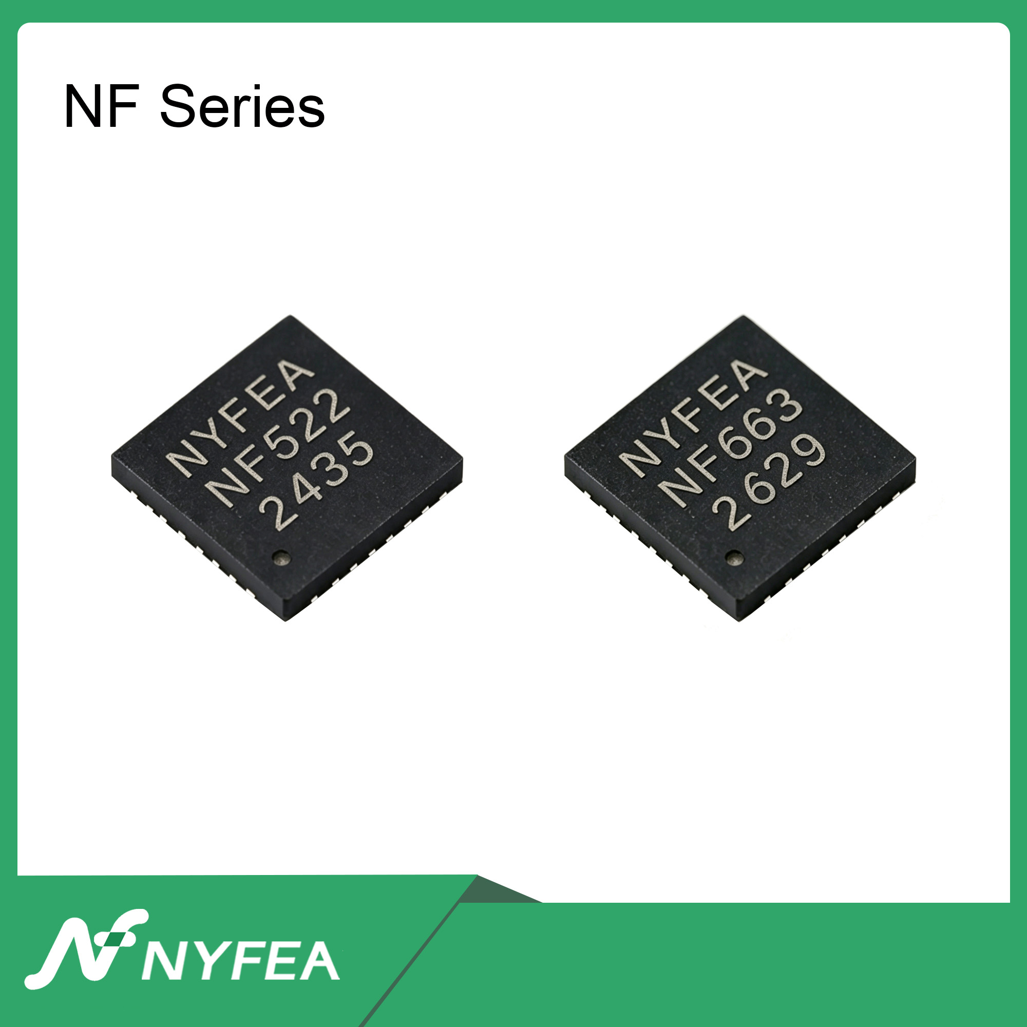
A 32-pin NF522 device must not be treated as automatically pin-to-pin compatible. The controlled NF522 document lists pins 7–9 as unused, whereas MFRC52202HN1 assigns them to MFIN, MFOUT and SVDD. The two devices also specify different supply ranges, host-interface limits and protocol capabilities. A redesign must compare every pin, rail, transaction, register and RF result.
How to read the engineering evidence
A value or function transcribed from the cited MFRC522 or NF522 technical source. Conditions and limits remain adjacent to the value.
A design recommendation derived from circuit behavior. It is useful for implementation but is not a guaranteed device specification.
A measurement or acceptance record required on the production-intent board. Passing one bench transaction is not equivalent to release qualification.
| Search question | Verified engineering answer |
|---|---|
| What is MFRC52202HN1? | The Version 2.0 MFRC522 13.56 MHz reader IC—not the name of a complete RC522 module. |
| What package is used? | HVQFN32, SOT617-1, documented as 5 × 5 × 0.85 mm with 0.50 mm terminal pitch. |
| Which host interfaces are available? | SPI up to 10 Mbit/s, I²C Standard-mode, Fast-mode and High-speed-mode operation, and serial UART up to 1228.8 kBd. |
| What clock is required? | A 27.12 MHz crystal connection or an externally generated 27.12 MHz clock at OSCIN. |
| Can a generic QFN32 part replace it? | No. Pin count does not prove pad geometry, pin assignment, electrical, register, firmware or RF compatibility. |
| Where does NF522 fit? | As an independent redesign candidate that adds documented Type B, ISO/IEC 15693 and LPCD capabilities, subject to full qualification. |
| What is the current lifecycle context? | NXP's product page identifies MFRC52202HN1 as End of Life and not recommended for new designs. Confirm current ordering status before any procurement or redesign decision. |
1. Start with the exact device—not the RC522 module nickname
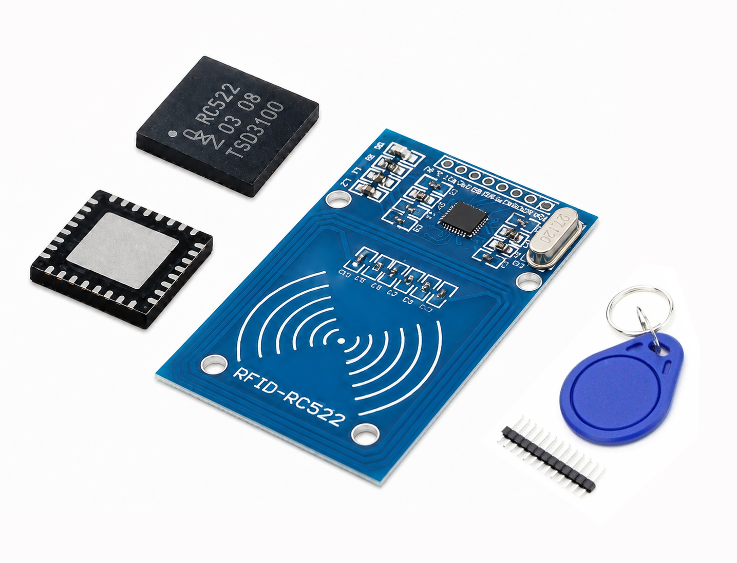
Search results for “MFRC52202HN1 pinout” often mix three different objects: the MFRC522 reader-IC family, the exact MFRC52202HN1 Version 2.0 device and complete blue RC522 modules. Only the exact device and controlled package data are suitable for a schematic symbol, PCB footprint, approved-vendor record or lifecycle decision.
A typical module adds a 27.12 MHz crystal, antenna coil, EMC and matching components, header, decoupling and sometimes level or power circuitry. Its eight-pin header is a module interface; it is not the MFRC52202HN1 chip pinout. Copying module header labels into an IC schematic is therefore a category error.
Lifecycle context: NXP's current product page marks MFRC52202HN1 as End of Life and not recommended for new designs. That status does not change the electrical facts below, but it changes sourcing risk and the purpose of the design review. Engineers addressing supply continuity should also use the MFRC52202HN1 lifecycle and NF522 migration guide.
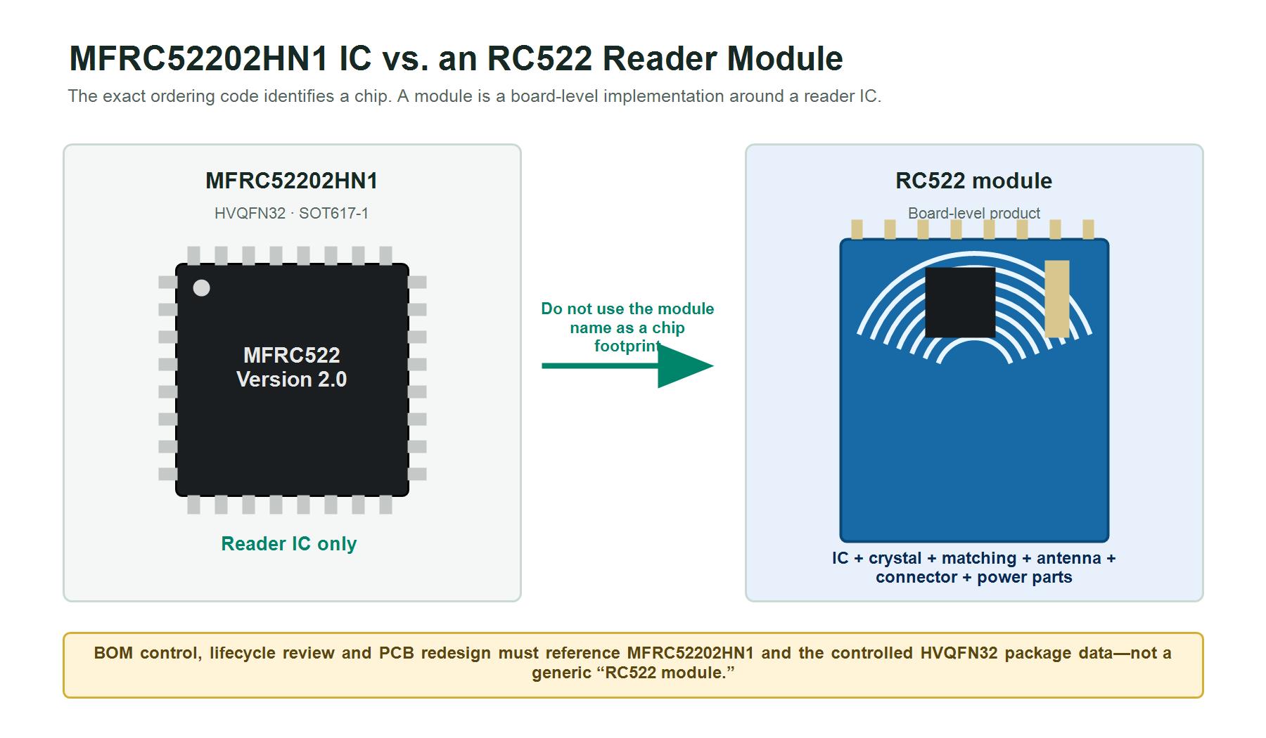
Design authority: build the symbol and footprint from the current controlled product and package documents. Treat marketplace module drawings, photos and pin labels only as documentation for that specific module.
2. MFRC52202HN1 pinout: all 32 terminals by function
The package drawing is a transparent top view. Pin 1 is identified by the package index mark. The pin table below separates supply, RF, oscillator/control and multiplexed host-interface functions so that a reviewer can audit every schematic connection.
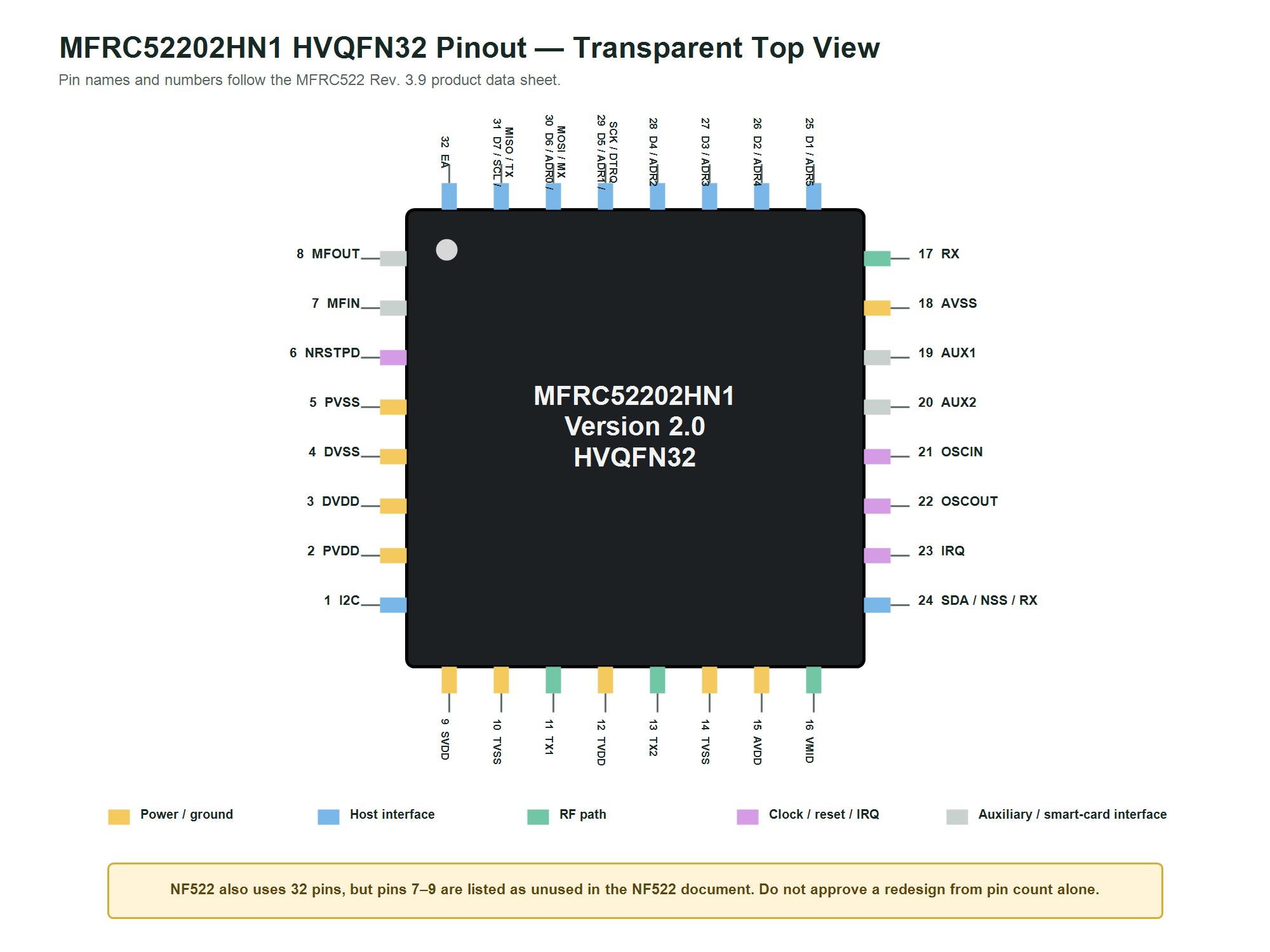
| Pin | Symbol | Design role |
|---|---|---|
| 1 | I2C | I²C-bus enable and host-interface selection input. |
| 2 | PVDD | Digital I/O pin supply. |
| 3 | DVDD | Digital core supply. |
| 4 | DVSS | Digital ground. |
| 5 | PVSS | Digital I/O pin-supply ground. |
| 6 | NRSTPD | Reset and hardware power-down input. LOW selects power-down; a positive edge initiates reset. |
| 7 | MFIN | MIFARE signal input. If unused, the data sheet requires connection to SVDD or PVSS. |
| 8 | MFOUT | MIFARE signal output. |
| 9 | SVDD | Supply for MFIN and MFOUT. |
| 10 | TVSS | Transmitter output-stage 1 ground. |
| 11 | TX1 | Modulated 13.56 MHz carrier output, transmitter 1. |
| 12 | TVDD | Supply for TX1 and TX2 transmitter stages. |
| 13 | TX2 | Modulated 13.56 MHz carrier output, transmitter 2. |
| 14 | TVSS | Transmitter output-stage 2 ground. |
| 15 | AVDD | Analog supply. |
| 16 | VMID | Internal analog reference. Use the specified external stabilization network. |
| 17 | RX | RF receive input from the antenna coupling network. |
| 18 | AVSS | Analog ground. |
| 19 | AUX1 | Auxiliary test output. |
| 20 | AUX2 | Auxiliary test output. |
| 21 | OSCIN | 27.12 MHz crystal-amplifier input or external clock input. |
| 22 | OSCOUT | Crystal-amplifier output. |
| 23 | IRQ | Interrupt-request output; electrical behavior is register-configurable. |
| 24 | SDA / NSS / RX | I²C data, SPI chip-select or UART receive/address input. |
| 25 | D1 / ADR_5 | Test port or I²C address bit 5. |
| 26 | D2 / ADR_4 | Test port or I²C address bit 4. |
| 27 | D3 / ADR_3 | Test port or I²C address bit 3. |
| 28 | D4 / ADR_2 | Test port or I²C address bit 2. |
| 29 | D5 / ADR_1 / SCK / DTRQ | Test port, I²C address bit 1, SPI clock or UART data-request signal. |
| 30 | D6 / ADR_0 / MOSI / MX | Test port, I²C address bit 0, SPI MOSI or UART MX signal. |
| 31 | D7 / SCL / MISO / TX | Test port, I²C clock, SPI MISO or UART transmit output. |
| 32 | EA | External-address and host-interface selection input. |
Pin-review questions that catch expensive errors
- Does the symbol use the transparent top-view numbering rather than a mirrored bottom view?
- Are both TVSS pins connected and placed close to the transmitter return path?
- Are all four primary supply domains and their grounds visible in the schematic review?
- Are interface-selection straps fixed to defined logic levels during power-on and hard reset?
- Are MFIN, MFOUT and SVDD handled according to the data sheet even if the smart-card interface is unused?
3. Power rails: values, equality rules and current conditions
The most important MFRC52202HN1 power rule is not simply “use 3.3 V.” AVDD, DVDD and TVDD must always be at the same voltage. PVDD must be equal to or lower than DVDD. These relationships apply throughout operation, including ramp and brownout behavior implemented by the final system.
| Domain | Minimum | Typical | Maximum | Adjacent condition |
|---|---|---|---|---|
| AVDD | 2.5 V | 3.3 V | 3.6 V | Must equal DVDD and TVDD. |
| DVDD | 2.5 V | 3.3 V | 3.6 V | Must equal AVDD and TVDD. |
| TVDD | 2.5 V | 3.3 V | 3.6 V | Must equal AVDD and DVDD; current depends strongly on the external TX circuit. |
| PVDD | 1.6 V | 1.8 V | 3.6 V | Must not exceed DVDD; sets digital-pin voltage behavior. |
| SVDD | 1.6 V | — | 3.6 V | Supplies MFIN/MFOUT. If unused, follow the data-sheet connection rule. |
| Ambient temperature | −25 °C | 25 °C | +85 °C | End-product limits and self-heating still require system verification. |
Performance condition: the MFRC522 data sheet warns that supply voltages below 3 V reduce performance, including achievable operating distance. A valid low-voltage design therefore needs RF performance measurements at the minimum production supply, not only successful register access.
Current figures are conditional, not one “chip current”
| Condition | Typical | Maximum | Why it matters |
|---|---|---|---|
| Hard power-down, total supplies | — | 5 µA | Board leakage and pull networks can dominate the finished-product result. |
| Soft power-down with RF detector on | — | 10 µA | Use the exact mode and detector setting when comparing standby claims. |
| DVDD digital current at 3 V | 6.5 mA | 9 mA | Host activity and operating state affect the complete system budget. |
| AVDD, receiver on at 3 V | 7 mA | 10 mA | Receiver state must be identified in every measurement. |
| TVDD, continuous wave | 60 mA | 100 mA | The typical value assumes the stated complementary driver and 40 Ω matched antenna condition. |
4. SPI, I²C and UART: select the interface before reset release
MFRC52202HN1 automatically detects its host interface after power-on or hard reset by sampling fixed logic levels on its selection pins. These straps must be stable before reset release. A firmware setting cannot repair an incorrectly strapped hardware interface after startup.
| Interface | Pin 1 I2C | Pin 32 EA | Active multiplexed signals | Documented maximum |
|---|---|---|---|---|
| Serial UART | LOW | LOW | Pin 24 RX; pin 31 TX; optional DTRQ/MX functions on pins 29/30. | 1228.8 kBd |
| SPI | LOW | HIGH | Pin 24 NSS, pin 29 SCK, pin 30 MOSI, pin 31 MISO. | 10 Mbit/s |
| I²C | HIGH | Address mode | Pin 24 SDA, pin 31 SCL; address inputs on pins 25–30 as configured. | 100 kBd in Standard-mode, 400 kBd in Fast-mode and 3.4 Mbit/s in High-speed mode |
Do not carry the I²C ceiling across to NF522
The reviewed NF522 document specifies I²C Fast mode up to 400 kbit/s. It does not establish MFRC522 High-speed-mode behavior at 3.4 Mbit/s. An existing MFRC52202HN1 host that uses I²C High-speed mode therefore requires a bus-speed and transaction redesign before NF522 evaluation.
5. Clock, reset and interrupt connections
27.12 MHz clock source
OSCIN and OSCOUT support the internal inverting amplifier for a 27.12 MHz quartz crystal. OSCIN can instead accept an externally generated 27.12 MHz clock. The data sheet lists a typical crystal load capacitance of 10 pF and a maximum ESR of 100 Ω; the selected crystal and external network still require oscillator-margin review.
- Place the crystal and associated components close to OSCIN and OSCOUT.
- Keep the oscillator loop compact and away from TX currents, fast host traces and switching regulators.
- Do not probe the oscillator with a high-capacitance method and then interpret the disturbed waveform as normal operation.
NRSTPD is both reset and hardware power-down
Holding NRSTPD LOW enables hardware power-down: internal current sinks are switched off, the oscillator is inhibited and input pins are disconnected from the outside world. A positive edge initiates reset. The MCU must not begin host transactions until the data-sheet timing and oscillator-start conditions have been met.
IRQ electrical behavior is configurable
IRQ reports enabled interrupt events. Register configuration determines polarity and whether the output behaves as a standard CMOS output or open-drain. The schematic pull network and MCU interrupt configuration must match the firmware setting.
6. RF transmitter, receive path and PCB layout
TX1 and TX2 drive the 13.56 MHz carrier through an EMC filter and matching network to the antenna. RX receives the coupled card response, while VMID provides the internal reference used by the receive path. Matching-component values are system values: they depend on antenna geometry, PCB stack-up, enclosure, nearby metal, cabling, component tolerance and target cards.
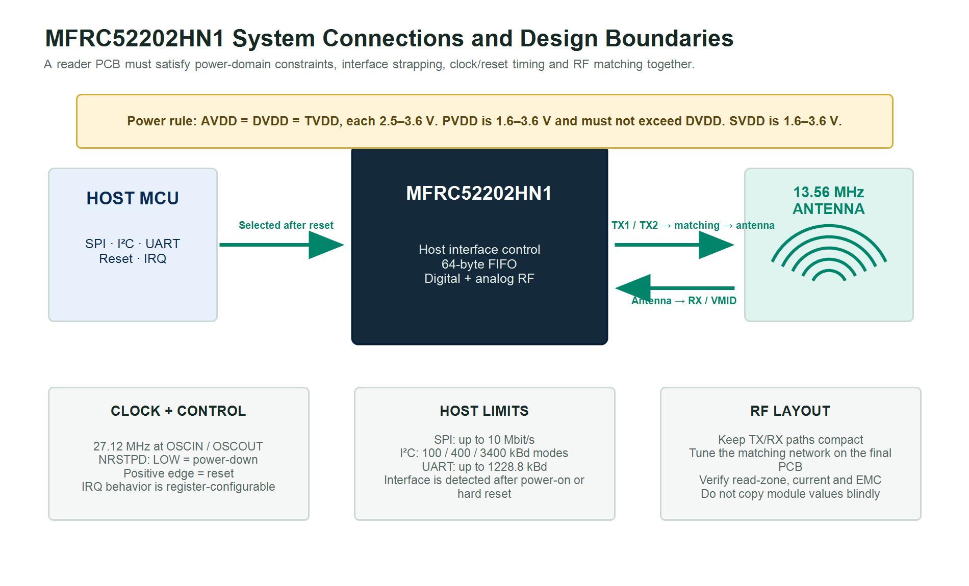
Layout priorities
- Keep the TX loop compact: route TX1, TX2, TVSS returns and the first EMC/matching components as a controlled local network.
- Protect RX and VMID: separate the sensitive receive/reference path from switching nodes and long digital traces.
- Decouple by function: place supply capacitors at the relevant domain pins with short return paths rather than relying on one remote bulk capacitor.
- Preserve antenna clearance: define copper, battery, display, shield and enclosure keep-outs from measured RF results.
- Tune on the final assembly: use a VNA or equivalent RF method on the production-intent PCB and repeat card tests in the final enclosure.
The MFRC522 data sheet’s typical application shows a complementary antenna connection and directs antenna tuning and matching work to the relevant application notes. It does not provide one universal matching BOM for every antenna.
7. HVQFN32 SOT617-1 package and land-pattern boundary
MFRC52202HN1 uses the SOT617-1 HVQFN32 package. Body dimensions D and E are each 4.9–5.1 mm, terminal pitch is 0.50 mm, and the exposed-pad dimensions are 2.95–3.25 mm. NXP states that connection of the bottom heatsink pad is not necessary and that an optional connection to DVSS is possible.
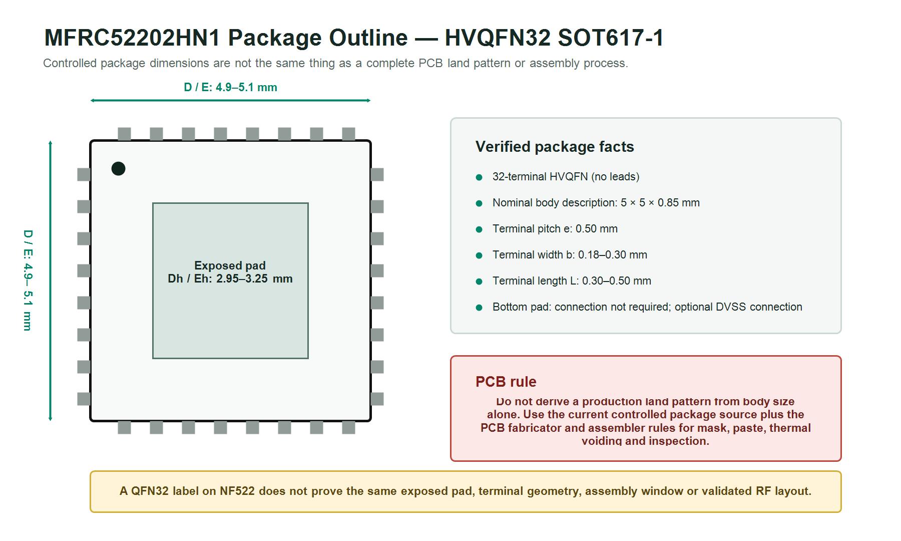
Common failure mode: “QFN32” describes a package family and pin count, not a guaranteed footprint. The body, pitch, terminal length, terminal width, exposed pad, pin-1 orientation and assembly window must all match the approved package source.
8. MFRC52202HN1 vs NF522: differences that affect a redesign
NF522 is a NYFEA multi-protocol reader IC that can be evaluated for a new design. Some pin positions and high-level functions resemble MFRC52202HN1, but the controlled documents also show material differences. The correct engineering conclusion is “candidate for redesign and qualification,” not “drop-in replacement.”
| Design item | MFRC52202HN1 documented baseline | NF522 documented baseline | Required action |
|---|---|---|---|
| Core reader modes | ISO/IEC 14443 Type A, MIFARE and NTAG | ISO/IEC 14443 Type A, Type B and ISO/IEC 15693 reader modes; M1 mode is also listed | Define the actual card set, data rates, security and licensing requirements. |
| Pins 7–9 | MFIN, MFOUT, SVDD | Listed as unused | Do not assume a one-to-one schematic or test-point transfer. |
| Core/transmitter supply | AVDD = DVDD = TVDD, 2.5–3.6 V | AVDD/DVDD 2.3–5.0 V; TVDD 2.0–5.0 V | Redesign rail conditions and decoupling from the selected device document; never apply NF522’s upper range to MFRC52202HN1. |
| Pin supply | PVDD 1.6–3.6 V and no higher than DVDD | PVDD 2.0–5.0 V | Recheck MCU I/O levels, straps and sequencing. |
| SPI | Up to 10 Mbit/s | Up to 12 Mbit/s; modes 0 and 3 are listed | Confirm framing, mode, timing and a production-safe rate. |
| I²C | Standard, Fast and High-speed modes up to 3.4 Mbit/s | Fast mode up to 400 kbit/s | Reduce or redesign an MFRC522 High-speed-mode host implementation. |
| UART | Up to 1228.8 kBd | 7.2 kbit/s to 1.2288 Mbit/s | Verify reset defaults, framing, register access and level conditions. |
| Low-power function | Hardware and software power-down; RF level detector is documented | Hard/Soft Power-Down plus dedicated LPCD registers and wake behavior | Measure whole-reader standby current, wake latency and false-wake performance. |
| Registers and driver | MFRC522 register and command architecture | NF522 register set includes device-specific base and extended registers | Keep separate low-level drivers until equivalence is proved function by function. |
| RF network | MFRC522-specific TX/RX conditions and matching guidance | NF522 application circuit specifies a device-specific antenna network and 40–50 Ω tuning note | Retune on the NF522 PCB; do not copy an MFRC522 module BOM. |
What can be reused safely?
Reuse product requirements, card fixtures, read-zone definitions, fault-policy states and manufacturing traceability. Treat the footprint, power tree, low-level driver, matching network and performance limits as items to be re-established.
Migration gates: conditions that block a release decision
| Gate | Release-blocking condition | Evidence needed to close the gate |
|---|---|---|
| G1 Pin map | Any MFRC52202HN1 function, including pins 7–9 or the exposed pad, is carried across without a documented NF522 disposition. | Signed 32-pin and exposed-pad difference matrix linked to both schematic revisions. |
| G2 Host bus | The existing design uses I²C above 400 kbit/s, or SPI/UART framing and reset behavior have not been captured. | Logic-analyzer records for reset, initialization, normal traffic, timeout and recovery at the released rate. |
| G3 Firmware | Any command, register, reset value, FIFO, timer, CRC, IRQ or error-recovery assumption is unmapped or untested. | Device-specific driver review plus automated transaction and fault-injection results. |
| G4 RF network | The MFRC52202HN1 antenna or matching BOM is copied to the NF522 board without measurement. | Production-intent impedance, tuning and read-zone records in the final enclosure. |
| G5 Acceptance | The only proof is a successful UID read from one card on an open bench. | Approved card matrix, orientation map, supply and temperature corners, recovery tests and defined pass/fail limits. |
9. Controlled NF522 redesign workflow
- Freeze the MFRC52202HN1 baseline. Archive the schematic, layout, antenna geometry, matching BOM, firmware revision, target-card set, current and read-zone data.
- Build a two-column pin audit. Include all 32 pins, exposed pad, unused-pin rules, host straps and test points. Record “same,” “different” or “not established”—never leave an assumed blank.
- Redesign power from operating conditions. Verify every rail, sequence, I/O level, decoupling path, field-on current, sleep mode and wake source.
- Implement an NF522-specific low-level driver. Keep commands, register definitions, FIFO, timer, CRC, interrupt and error recovery behind a common application API.
- Capture real host transactions. Use a logic analyzer for reset, identification, first configuration write, card polling, timeout and recovery.
- Retune the RF network. Measure the assembled reader in its final mechanical stack rather than copying a reference-module capacitor set.
- Run controlled A/B testing. Use the same cards, positions, orientations, supply corners, temperature points, noise states and acceptance limits for both boards.
Recommended firmware boundary
Application states and product policy
                │
        Common reader API
          ┌─────┴─────┐
          │           │
 MFRC522 driver   NF522 driver
 register map A   register map B
A common application API can preserve product behavior while the device-specific layers remain independently testable. This structure avoids disguising an unverified register assumption as “driver compatibility.”
10. Evidence required before production release
The following verification scale prevents a prototype demonstration from being reported as production qualification. A project advances only when the evidence at the current level is repeatable and traceable to hardware, firmware, fixture and test-condition revisions.
| Level | What has been established | What has not yet been established |
|---|---|---|
| V0 Document review | Part identity, lifecycle context, pin map, operating conditions, interfaces and package sources are controlled. | No board behavior has been demonstrated. |
| V1 Bench communication | Reset, device access and at least one card transaction work on an identified prototype. | RF margin, recovery, environmental corners and manufacturing variation remain unknown. |
| V2 Functional A/B | Required card operations and read-zone criteria pass against the frozen MFRC52202HN1 baseline. | Corner, stress and production-process evidence is incomplete. |
| V3 Corner and recovery | Supply, temperature, interference, fault recovery, low-power and mechanical conditions meet defined limits. | Factory repeatability and release traceability are not yet approved. |
| V4 Production release | Design, manufacturing test, golden units, change control and qualification records are approved. | Only future change-control and field-monitoring obligations remain. |
| Evidence group | Minimum record | Acceptance decision |
|---|---|---|
| Electrical | All rails, ramp/brownout behavior, field-on current, standby current and I/O levels | Every value remains inside the selected device and product limits with margin. |
| Digital interface | Reset-to-first-command capture; normal read/write; timeout and bus-error recovery | No undocumented timing dependency or required power cycle. |
| Functional cards | Required card technologies, data rates, authentication and representative lot variation | All product use cases pass—not only UID reading. |
| RF | Antenna impedance/matching record, read-zone map, orientation, enclosure and interference states | Coverage and margin meet the product requirement. |
| Low power | Entry current, wake current, latency, false-wake rate and state retention | Whole-system power and response requirements are met. |
| Environment | Supply corners, temperature, tolerances and representative mechanical builds | Results meet released product limits across the qualification matrix. |
| Manufacturing | AOI/X-ray criteria as applicable, test points, golden units, firmware/hardware revision traceability | The factory can distinguish assembly, digital and RF failures. |
One card read on an open bench proves only that one transaction occurred. Production approval requires repeatable evidence for startup, recovery, RF coverage, environmental corners and manufacturing variation.
11. Engineering FAQs
What is the MFRC52202HN1 pinout?
MFRC52202HN1 uses 32 HVQFN terminals. Pins 1–6 cover interface selection, supplies, grounds and reset; pins 7–9 are MFIN, MFOUT and SVDD; pins 10–18 form the main transmitter, analog and receive path; pins 19–23 cover auxiliary, clock and IRQ functions; pins 24–32 multiplex SPI, I²C, UART, address and test functions.
Is MFRC52202HN1 the same as an RC522 module?
No. MFRC52202HN1 is a reader IC. An RC522 module is a board-level implementation that normally includes a reader IC, crystal, antenna, matching network, connector and support components.
Is MFRC52202HN1 End of Life?
NXP's current MFRC52202HN1 product page identifies the device as End of Life and not recommended for new designs. Lifecycle and ordering information can change, so verify the current manufacturer status and authorized-channel availability when making a procurement or redesign decision.
What package does MFRC52202HN1 use?
It uses the SOT617-1 HVQFN32 package, documented as a 5 × 5 × 0.85 mm body with 0.50 mm terminal pitch. Use the current controlled package information for the production footprint.
Can MFRC52202HN1 operate from 5 V?
No. The recommended operating maximum for AVDD, DVDD and TVDD is 3.6 V. Do not confuse this with the wider operating ranges listed for a different reader IC.
Which MFRC52202HN1 interface is fastest?
The data sheet lists I²C High-speed mode up to 3.4 Mbit/s, SPI up to 10 Mbit/s and serial UART up to 1228.8 kBd. The appropriate interface and operating rate depend on MCU support, routing, pull-ups and timing margin.
Does QFN32 mean NF522 is pin-compatible?
No. QFN32 is not a complete compatibility statement. Pin functions, body and exposed-pad geometry, supplies, reset behavior, host transactions, registers, firmware and RF network all require comparison.
What is the most important MFRC52202HN1-to-NF522 pin difference?
The reviewed documents show MFRC52202HN1 pins 7–9 as MFIN, MFOUT and SVDD, while the NF522 pin table lists pins 7–9 as unused. This alone is sufficient to reject compatibility based only on pin count.
Can an MFRC522 driver be reused unchanged with NF522?
Do not assume unchanged reuse. Compare commands, register addresses and reset values, FIFO behavior, timing, CRC, IRQ and error recovery. A separate NF522 low-level driver behind a common reader API is the safer structure.
Does the MFRC52202HN1 matching network transfer to NF522?
Not as a guaranteed BOM. Antenna geometry may be retained as an initial experiment, but the matching and EMC network must be measured and tuned on the NF522 PCB in the final mechanical environment.
Controlled technical sources
MFRC522 source: NXP MFRC522 product data sheet, Rev. 3.9, 27 April 2016. Verify the current document revision and ordering status before design approval.
Lifecycle source: NXP MFRC52202HN1 product page, checked on 26 August 2026. Recheck this live source when making a purchasing decision.
NF522 source: NYFEA NF522 technical data supplied with the product evaluation package. The cited Type A, Type B, ISO/IEC 15693, host-interface, low-power, pin and operating-condition facts are taken from that controlled document. Confirm the current released revision before schematic approval.
Trademark and relationship notice: MFRC522, MIFARE, NTAG, NXP and related product names are identifiers or marks of their respective owners. NF522 is a NYFEA product. NYFEA and NF522 are not affiliated with, endorsed by or sponsored by NXP. This comparison is provided only for engineering selection and redesign assessment.
Evaluating an NF522 redesign for an MFRC52202HN1 board?
Send NYFEA the approved card list, host interface, rail plan, existing pin map, antenna dimensions, enclosure stack and measured MFRC52202HN1 baseline. The useful first deliverable is a controlled difference matrix—not a one-line “drop-in” claim.